A210 SODIMM V1 Baseboard
The A210 SODIMM V1 baseboard establishes the foundation for a basic development kit by connecting to a PC via serial port, USB, and Ethernet. To build a more comprehensive development or demo environment, you will need the following additional components:
- A display
- An audio source and speakers
- USB 2.0/3.0 devices
- Storage media, such as a USB flash drive or a microSD (TF) card.
Features
A210 SODIMM V1 includes the following features.
- One 2x10-pin 2.54mm header provides expansion for a QSPI interface.
- One 2x10-pin 2.54mm header provides expansion for a SDIO/UART interface.
- Two RJ45 Ethernet ports supporting 10/100/1000 Mbps in full-/half-duplex mode.
- One full-featured USB 3.1 port with DP ALT mode support.
- One USB 2.0 Type-C port for flashing.
- One USB 2.0 Type-A port.
- One PCIe 3.0 x4 port.
- One HDMI 2.0 port.
- One RS232 port.
- One RS485 port.
- One CAN port.
- Analog audio input and output ports.
- One MIPI-DSI expansion port.
- One 2-lane MIPI-CSI Board-to-Board (B2B) connector.
- One 4-lane MIPI-CSI Board-to-Board (B2B) connector.
Hardware Introduction
Connectors
A210 SODIMM V1 reserves a wealth of peripheral connectors.
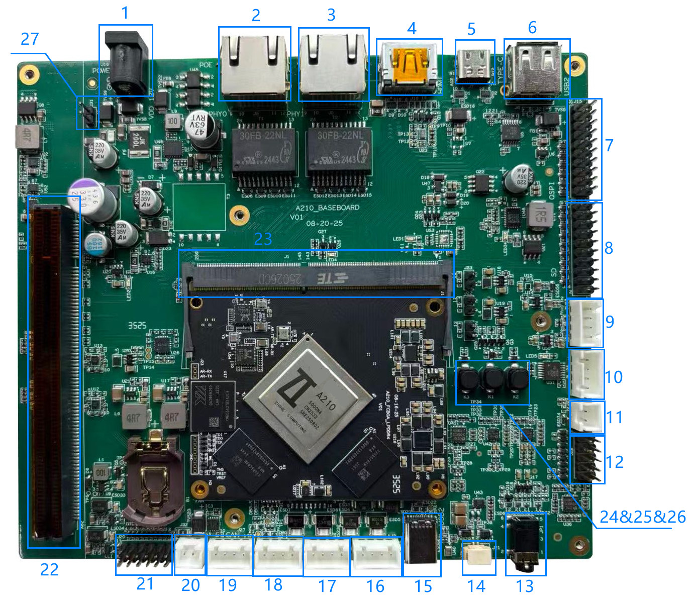
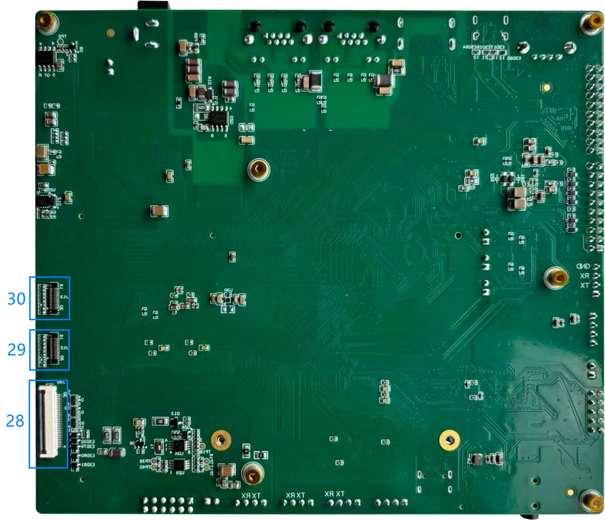
The description of A210 SODIMM V1 connector is as follows.
| NO. | Description |
|---|---|
| 1 | 12V DC Input |
| 2 | RJ45 connector with PoE Support |
| 3 | RJ45 connector |
| 4 | HDMI connector |
| 5 | USB3.1 Type-C connector with DP support |
| 6 | USB2.0 Type-A connector |
| 7 | QSPI0 expansion header |
| 8 | SDIO+UART5 expansion header |
| 9 | PD IC Serial debug header |
| 10 | PCle X1 sideband signals header |
| 11 | PCle RC/EP switch |
| 12 | Reserved GPIO expansion header |
| 13 | 3.5mm audio jack |
| 14 | Speaker expansion header |
| 15 | USB2.0 Type-C connector for flashing |
| 16 | UART8 to RS-485 port |
| 17 | UART8 to RS-232 port |
| 18 | A210 debug UART header |
| 19 | CAN0 interface |
| 20 | 12V fan header |
| 21 | PCle add-in card header |
| 22 | PCle slot |
| 23 | sodimm socket |
| 24 | Power button |
| 25 | Flash button |
| 26 | Reset button |
| 27 | Auxiliary 12V input header |
| 28 | MIPI DSI expansion connector |
| 29 | MIPI-CSI1 X2 Board-to-Board (B2B) expansion connector |
| 30 | MIPI-CSI0 X4 Board-to-Board (B2B) expansion connector |
QSPI0 Expansion Header
The baseboard provides a QSPI0 interface. Users can design and verify based on this header's pinout to connect an external QSPI Flash or TPM device.
- 2.54mm pin pitch header.
- Power pins: 3V3(1.5A max current), 1V8(1.5A max current).
- The power rail is shared with the SDIO interface. Ensure the total current draw does not exceed the specified limits when both interfaces are in use.
| pin_net | pin | pin | pin_net |
|---|---|---|---|
| GND | 1 | 2 | QSPI0_CSN0 |
| GND | 3 | 4 | QSPI0_SCLK |
| GND | 5 | 6 | QSPI0_D0_MOSI |
| GND | 7 | 8 | QSPI0_D1_MISO |
| GND | 9 | 10 | QSPI0_D2_WP |
| GND | 11 | 12 | QSPI0_D3_HOLD |
| GND | 13 | 14 | NC |
| GND | 15 | 16 | NC |
| GND | 17 | 18 | 3V3 |
| GND | 19 | 20 | 1V8 |
SDIO+UART5 Expansion Header
The header is primarily intended for SDIO interface chip validation.
- 2.54mm pin pitch header.
- Validation of the TF card and 6222B-SRC WiFi chip via an add-in card has been completed.
- The header can be used as general-purpose GPIOs if no add-in card is connected. For details, see General-purpose GPIO Signal Description.
- A customized add-in card is required if the users need to validate other WiFi chips or SD card components.
- Power pins: 3V3(1.5A max current), 1V8(1.5A max current)
- The power rail is shared with the SDIO interface. Ensure the total current draw does not exceed the specified limits when both interfaces are in use.
| pin_net | pin | pin | pin_net |
|---|---|---|---|
| SDIO_DAT3 | 1 | 2 | 3V3 |
| SDIO_CMD | 3 | 4 | 1V8 |
| SDIO_CLK | 5 | 6 | GND |
| SDIO_DAT2 | 7 | 8 | BT_EN AOGPIO1_4 |
| SDIO_DAT0 | 9 | 10 | BT_WAKE_HOST AOGPIO0_30 |
| SDIO_DAT1 | 11 | 12 | HOST_WAKE_BT GPIO0_17 |
| NC | 13 | 14 | UART5_TXD |
WL_EN GPIO0_14 | 15 | 16 | UART5_RXD |
WL_WAKE_HOST AOGPIO1_3 | 17 | 18 | UART5_CTSN |
| GND | 19 | 20 | UART5_RTSN |
PD IC Serial Debug Header
The debug UART for MPF52002 PD controller. Not recommended for use.
- Type: XH2.54-4P.
- For any power delivery (fast charging) requirements, please contact our technical support for evaluation.
| pin | pin_net |
|---|---|
| 1 | NC |
| 2 | TX |
| 3 | RX |
| 4 | GND |
PCIe X1 Sideband Signals Header
The baseboard provides PCIe x1 sideband signals for slot bifurcation when used with an add-in card.
- Type: XH2.54-4P.
- Please connect according to the PCIe specification. For details, please see PCIe Mode Configuration.
| pin | pin_net |
|---|---|
| 1 | Prsnt |
| 2 | Wake |
| 3 | Clkreq_n |
| 4 | Perst_n |
Reserved GPIO Expansion Header
General-purpose GPIO expansion header.
- 2.54mm pin pitch header.
- ADC_CH1: as an ADC input channel, support a voltage range of 0 to 1.8V.
- Power pins: 5V/3V3/1V8 provide board-level power and are not current-limited. Take care to prevent short circuits.
| pin_net | pin | pin | pin_net |
|---|---|---|---|
| GPIO1_16 | 1 | 2 | 5V |
| GPIO2_16 | 3 | 4 | 3V3 |
| GPIO1_1 | 5 | 6 | 1V8 |
| ADC_CH1 | 7 | 8 | GPIO2_7 |
| GND | 9 | 10 | GND |
UART8 to RS-485 Port
General-purpose RS-485 port for use as required.
- Type: XH2.54-4P.
- Please notice that the RS-485 and RS-232 functions are mutually exclusive and cannot be used simultaneously.
| pin | pin_net |
|---|---|
| 1 | RS485_B |
| 2 | RS485_A |
| 3 | NC |
| 4 | NC |
UART8 to RS-232 Port
General-purpose RS-232 port for use as required.
- Type: XH2.54-4P.
- Please notice that the RS-485 and RS-232 functions are mutually exclusive and cannot be used simultaneously.
| pin | pin_net |
|---|---|
| 1 | NC |
| 2 | NC |
| 3 | TX |
| 4 | RX |
A210 Debug UART Header
- Type: XH2.54-4P.
- Power pins: 3V3.
| pin | pin_net |
|---|---|
| 1 | NC |
| 2 | TX |
| 3 | RX |
| 4 | GND |
CAN0 Interface
- Type: XH2.54-4P.
- Power pins: 1V8.
| pin | pin_net |
|---|---|
| 1 | NC |
| 2 | TX |
| 3 | RX |
| 4 | GND |
PCIe Add-in Card Header
The baseboard provides the header to communicate with the I/O controller when connecting to a PCIe add-in card. If no add-in card is present, these pins can be configured as GPIO.
- Type: XH2.54-4P.
- Power pins: Supplies 5V board-level power. No current-limited.
- I2C interface: Operates at 1.8V logic level.
| pin_net | pin | pin | pin_net |
|---|---|---|---|
| 5V | 1 | 2 | NC |
| PCIe_EXP_INTB | 3 | 4 | SATA_EXP_INTB |
| I2C7_SCL | 5 | 6 | I2C_SCL_ID0 |
| I2C7_SDA | 7 | 8 | I2C_SDA_ID1 |
| NC | 9 | 10 | I2C4_SCL |
| GND | 11 | 12 | I2C4_SDA |
MIPI DSI Expansion Connector
- Type: Flexible Printed Circuit (FPC) connector.
- An adapter board can be used for screen validation.
- Pins labeled for TP can also be repurposed for other functions.
- Power Rails: 3V3_TP (3.3V supply with 1.5A current limit), 3V3_D (3.3V supply with 1.5A current limit).
- LED_K/A: Backlight Power, up to 36V, 100 mA.
| pin | pin_net |
|---|---|
| 1 | 3V3_TP |
| 2 | TP_I2C_SDA |
| 3 | TP_I2C_SCL |
| 4 | TP_RST |
| 5 | TS_INT |
| 6 | GND |
| 7 | DISP_RST |
| 8 | GND |
| 9 | 3V3_D |
| 10 | 3V3_D |
| 11 | GND |
| 12 | MIPI_DSI0_DAT2N |
| 13 | MIPI_DSI0_DAT2P |
| 14 | GND |
| 15 | MIPI_DSI0_DAT1P |
| 16 | MIPI_DSI0_DAT1N |
| 17 | GND |
| 18 | MIPI_DSI0_CLKP |
| 19 | MIPI_DSI0_CLKN |
| 20 | GND |
| 21 | MIPI_DSI0_DAT0N |
| 22 | MIPI_DSI0_DAT0P |
| 23 | GND |
| 24 | MIPI_DSI0_DAT3N |
| 25 | MIPI_DSI0_DAT3P |
| 26 | GND |
| 27 | LED_K |
| 28 | LED_K |
| 29 | LED_A |
| 30 | LED_A |
MIPI-CSI1 X2 B2B Expansion Connector
The baseboard provides a 2-lane MIPI-CSI interface.
- Power Management:
- Supply voltages are controlled and current-limited by a PMIC (WL2866).
- 2.8V_AVDD/1.8V_AVDD with 300mA max.each, 1.2V_DVDD/1.8V_DVDD with 820mA max. each.
- Type: BM20B(0_8)-30DS-0_4V(51).
- Validating other camera modules requires a small adapter board for signal bridging.
| pin_net | pin | pin | pin_net |
|---|---|---|---|
| PWDN | 1 | 30 | NC |
| 2.8V_AVDD | 2 | 29 | NC |
| ID | 3 | 28 | GND |
| 1.8V_DOVDD | 4 | 27 | NC |
| 1.2V_DVDD | 5 | 26 | NC |
| 1.2V_DVDD | 6 | 25 | GND |
| GND | 7 | 24 | MIPI_CSI1_A_DAT1N |
| MCLK | 8 | 23 | MIPI_CSI1_A_DAT1P |
| GND | 9 | 22 | GND |
| SDA | 10 | 21 | MIPI_CSI1_A_DAT0N |
| SCL | 11 | 20 | MIPI_CSI1_A_DAT0P |
| RST | 12 | 19 | GND |
| FSIN | 13 | 18 | MIPI_CSI1_A_CLKN |
| 1.8V_AVDD | 14 | 17 | MIPI_CSI1_A_CLKP |
| GND | 15 | 16 | GND |
MIPI-CSI0 X4 B2B Expansion Connector
The baseboard provides a 4-lane MIPI-CSI interface.
- Power Management:
- Supply voltages are controlled and current-limited by a PMIC (WL2866).
- 2.8V_AVDD/1.8V_AVDD with 300mA max.each, 1.2V_DVDD/1.8V_DVDD with 820mA max. each.
- Type: BM20B(0_8)-30DS-0_4V(51).
- Validating other camera modules requires a small adapter board for signal bridging.
| pin_net | pin | pin | pin_net |
|---|---|---|---|
| PWDN | 1 | 30 | MIPI_CSI0_B_DAT1N |
| 2.8V_AVDD | 2 | 29 | MIPI_CSI0_B_DAT1P |
| ID | 3 | 28 | GND |
| 1.8V_DOVDD | 4 | 27 | MIPI_CSI0_B_DAT0N |
| 1.2V_DVDD | 5 | 26 | MIPI_CSI0_B_DAT0P |
| 1.2V_DVDD | 6 | 25 | GND |
| GND | 7 | 24 | MIPI_CSI0_A_DAT1N |
| MCLK | 8 | 23 | MIPI_CSI0_A_DAT1P |
| GND | 9 | 22 | GND |
| SDA | 10 | 21 | MIPI_CSI0_A_DAT0N |
| SCL | 11 | 20 | MIPI_CSI0_A_DAT0P |
| RST | 12 | 19 | GND |
| FSIN | 13 | 18 | MIPI_CSI0_A_CLKN |
| 1.8V_AVDD | 14 | 17 | MIPI_CSI0_A_CLKP |
| GND | 15 | 16 | GND |
Modules Introduction
BOOT_SEL Configuration
| Pin | Baseboard GPIO Pin | Function | Baseboard Configuration |
|---|---|---|---|
| BOOT_SEL0/AOGPIO0_1 | BOOT_SEL0 | Boot Mode Select | R65 Pull-up, R70 NC |
| BOOT_SEL1/AOGPIO0_2 | BOOT_SEL1 | Boot Mode Select | R64 NC, R69 Pull-down |
| BOOT_SEL2/AOGPIO0_23 | BOOT_SEL2 | Boot Mode Select | R494 NC, R495 Pull-down |
Boot Mode Settings
| ID | BOOT_SEL2 | BOOT_SEL1 | BOOT_SEL0 | Boot Mode Setting |
|---|---|---|---|---|
| 0 | 0 | 0 | 0 | CCTBoot/USB Download |
| 1 | 0 | 0 | 1 | eMMC Boot (baseboard default) |
| 2 | 0 | 1 | 0 | SPI NOR Boot, QSPI1, CS0 |
| 3 | 0 | 1 | 1 | SPI NAND boot, QSPI1, CS0 |
| 4 | 1 | 0 | 0 | Forced CCTBoot |
| 5 | 1 | 0 | 1 | SD Boot, SDIO0 |
| 6 | 1 | 1 | 0 | SPI NOR Boot, QSPI0, CS0 |
| 7 | 1 | 1 | 1 | SPI NAND boot, QSPI0, CS0 |
Note: If you need to change the boot mode, modifications must be made by soldering.
PCIe Mode Configuration
| Pin | Baseboard GPIO Pin | Function | Baseboard Configuration |
|---|---|---|---|
| AOGPIO1_8/PCIe_RC_EP_SEL | PCIe_RC_EP_SEL | PCIe Mode Select | J29 1: RC mode, pin left floating. 0: EP mode, install a jumper shunt. |
The baseboard supports a PCIe 3.0 x4 interface with lane bifurcation capability. The available configurations are as follows:
| PHY | PHY0(x2) | PHY1(x2) | ||
| lane# | 0 | 1 | 2 | 3 |
| NO. | Configuration | |||
| 1 | X4 | |||
| 2 | X2 | X1 | ||
| 3 | X2 | SATA | SATA | |
| 4 | X1 | X1 | SATA | SATA |
- SOC integrates 2 PCIe controllers and 2 SATA controllers.
- PCIe Controllers: supports PCIE3.0 protocol.
- PHY0 Controllers: supports PCIe in both RC and EP modes. Lane configurations: X4, X2, X1.
- PHY1 Controllers: supports RC mode only. Lane configurations: X1 only.
- SATA Controllers: supports SATA3.0 protocol.
- The baseboard is equipped with a PCIe x16 mechanical slot. However, the SoC's electrical support is limited to PCIe x4 lanes.
I2C Address Assignment
The chips used at the board level are shown in the figure below.
Note: Ensure there are no I2C address conflicts when adding devices via reserved interfaces.
| I2C BUS | Device | I2C Address |
|---|---|---|
| AOI2C | AW9523 | 0100000 |
| AW9523 | 0100001 | |
| MP52002 | 0x27 | |
| TP | 0010100/1011101 | |
| I2C4 | PCIE_SMBUS | |
| SIT91211 | 0010000 | |
| RTC | 1010001 | |
| I2C5 | aud0_ADC | 1000000 |
| AUD0_DAC | 0001000 | |
| aud1_ADC | 1000001 | |
| AUD1_DAC | 0001001 | |
| AUD1_PA | 1011011 | |
| I2C6 | sensor0 | |
| sensor0_PWR | 0101000 | |
| PCIE Add-in Card IO0 | 0100000 | |
| I2C7 | sensor1 | |
| sensor1_PWR | 0101000 | |
| PCIE Add-in Card IO1 | 0100000 |
Power Control Description
| Pin | Controller | Net Name | Description |
|---|---|---|---|
| AOGPIO0_29 | A210 | POWER_5V_EN | VDD_5V enable signal. 1: enable, 0: disable. |
| AOGPIO0_26 | A210 | POWER_3V3_EN | VDD_3V3 enable signal. 1: enable, 0: disable. |
| GPIO0_27 | A210 | USBTypeC_PWREN | Reserved USB3.1 Type-C power output signal. Typically controlled by the PD chip. |
| P00 | AW9535 | PCIe_BAT_EN | 12V boost circuit(battery) enable signal. 1: enable, 0: disable. |
| P01 | AW9535 | AUDIO_3V3_PWREN | Audio 3V3 power enable signal. 1: enable, 0: disable. |
| P02 | AW9535 | AUDIO_1V8_PWREN | Audio 1V8 power enable signal. 1: enable, 0: disable. |
| P03 | AW9535 | MIPI_CSI0_PWREN | Camera power enable signal. 1: enable, 0: disable. It is recommended to keep this low and control output via the I2C chip. |
| P04 | AW9535 | MIPI_CSI1_PWREN | Camera power enable signal. 1: enable, 0: disable. It is recommended to keep this low and control output via the I2C chip. |
| P05 | AW9535 | MIPI_TP_PWREN | Screen TP power enable signal. 1: enable, 0: disable. |
| P06 | AW9535 | PCIe_3V3_EN | PCIe slot 3V3 power enable signal. 1: enable, 0: disable. |
| P07 | AW9535 | PCIe_12V_EN | PCIe slot 1V8 power enable signal. 1: enable, 0: disable. |
| P10 | AW9535 | USBCON_PWREN | USB2.0 Type-A port 5V power enable signal. 1: enable, 0: disable. |
| P11 | AW9535 | USBCON1_PWREN | USB2.0 Type-C port 5V power enable signal. 1: enable, 0: disable. |
| P12 | AW9535 | PCIe_3V3_AUX_EN | PCIe slot AUX_3V3 power enable signal. 1: enable, 0: disable. |
| P13 | AW9535 | SDIO_3V3_PWREN | SDIO header 3V3 power enable signal. 1: enable, 0: disable. |
| P14 | AW9535 | SDIO_1V8_PWREN | SDIO header 1V8 power enable signal. 1: enable, 0: disable. |
| P15 | AW9535 | SIT91211_3V3_EN | Chip SIT91211 3V3 power enable signal. 1: enable, 0: disable. |
| P16 | AW9535 | MIPI_DSI_PWREN | Screen 3V3 power enable signal. 1: enable, 0: disable. |
| P17 | AW9535 | BL_EN | Screen backlight power enable signal. 1: enable, 0: disable. |
General-purpose GPIO Signal Description
| Pin | Controller | Net Name | Description |
|---|---|---|---|
| AOGPIO1_9 | A210 | PCIE_X4_RC_WAKEN | Used as WAKEN signal when the PCIe X4 operates in RC mode. |
| AOGPIO1_7 | A210 | TypeC_DPTX_AUX_PUPDCTL1 | Pull-up/pull-down control signal for the AUX channel when the Type-C interface carries DP signals. |
| AOGPIO0_30 | A210 | TypeC_DPTX_AUX_PUPDCTL2 | Pull-up/pull-down control signal for the AUX channel when the Type-C interface carries DP signals. |
| AOGPIO1_1 | A210 | PCIE_EXP_INTB | With PCIe add-in card: int signal from the I/O expansion chip. Without PCIe add-in card: Reserved GPIO. |
| AOGPIO0_28 | A210 | SATA_EXP_INTB | With SATA add-in card: int signal from the I/O expansion chip. Without PCIe add-in card: Reserved GPIO. |
| AOGPIO0_27 | A210 | RTC_INT | int signal from the RTC chip. |
| GPIO0_14 | A210 | WL_EN | With Wi-Fi/BT module: WiFi enable signal. Without module: Reserved GPIO. |
| GPIO1_1 | A210 | GPIO1_1 | Reserved GPIO. |
| AOGPIO1_2 | A210 | IO0_INT | int signal from the AW9535 |
| AOGPIO1_3 | A210 | WL_WAKE_HOST | With Wi-Fi/BT module: WiFi wake-up signal to the host. Without module: Reserved GPIO. |
| AOGPIO1_4 | A210 | BT_EN | With Wi-Fi/BT module: Bluetooth enable signal. Without module: Reserved GPIO. |
| AOGPIO0_30 | A210 | BT_WAKE_HOST | With Wi-Fi/BT module: Bluetooth wake-up signal to the host. Without module: Reserved GPIO. |
| AOGPIO1_0 | A210 | TS_INT | Interrupt signal from the TP |
| AOGPIO1_6 | A210 | IO1_INT | int signal from the AW9535 |
| GPIO1_16 | A210 | GPIO1_16 | Reserved GPIO. |
| GPIO0_16 | A210 | HP_DET_L | Headphone insertion detection. |
| ADC_VIN_CH0 | A210 | ADC_VIN_CH0 | Headphone microphone input. |
| ADC_VIN_CH1 | A210 | ADC_VIN_CH1 | Reserved GPIO. |
| GPIO3_0 | A210 | MIPI_CSI0_MCLK | MCLK signal for the sensor. |
| GPIO3_1 | A210 | MIPI_CSI1_MCLK | MCLK signal for the sensor. |
| GPIO3_2 | A210 | UART8_TXD | UART signal. |
| GPIO3_3 | A210 | UART8_RXD | UART signal. |
| GPIO2_21 | A210 | UART8_CTSN | UART signal. |
| GPIO2_22 | A210 | UART8_RTSN | UART signal. |
| GPIO3_4 | A210 | TP_RST | Reset signal for the touch panel. |
| GPIO2_17 | A210 | GPIO2_17 | Reserved GPIO. |
| GPIO2_18 | A210 | UART5_TXD | UART signal. |
| GPIO2_19 | A210 | UART5_RXD | UART signal. |
| GPIO3_9 | A210 | UART5_CTSN | UART signal. |
| GPIO3_10 | A210 | UART5_RTSN | UART signal. |
| GPIO2_0 | A210 | UART4_TXD | UART signal. |
| GPIO2_1 | A210 | UART4_RXD | UART signal. |
| GPIO2_2 | A210 | I2S1_BCLK | Audio I2S signal. |
| GPIO2_3 | A210 | I2S1_LRCK | Audio I2S signal. |
| GPIO2_4 | A210 | I2S1_DIN | Audio I2S signal. |
| GPIO2_5 | A210 | I2S1_DOUT | Audio I2S signal. |
| GPIO2_6 | A210 | I2S1_MCLK | Audio I2S signal. |
| GPIO2_7 | A210 | GPIO2_7 | Reserved GPIO. |
| GPIO2_8 | A210 | I2C6_SCL | I2C signal. |
| GPIO2_9 | A210 | I2C6_SDA | I2C signal. |
| GPIO2_10 | A210 | I2C7_SCL | I2C signal. |
| GPIO2_11 | A210 | I2C7_SDA | I2C signal. |
| GPIO2_12 | A210 | PWM1_CH2 | Screen backlight control signal. |
| GPIO2_25 | A210 | HDMI_CEC | HDMI CEC signal. |
| GPIO2_30 | A210 | HDMI_SCL | HDMI I2C signal. |
| GPIO2_31 | A210 | HDMI_SDA | HDMI I2C signal. |
| GPIO2_26 | A210 | I2C4_SCL | I2C signal. |
| GPIO2_27 | A210 | I2C4_SDA | I2C signal. |
| GPIO2_28 | A210 | I2C5_SCL | I2C signal. |
| GPIO2_29 | A210 | I2C5_SDA | I2C signal. |
| GPIO2_16 | A210 | GPIO2_16 | Reserved GPIO. |
| AOGPIO0_8 | A210 | AOI2C1_SCL | I2C signal. |
| AOGPIO0_9 | A210 | AOI2C1_SDA | I2C signal. |
| P00 | AW9535 | CSI1_PWDN | Control signal for MIPI-CSI. |
| P01 | AW9535 | CSI1_RST | Reset signal for MIPI-CSI. |
| P02 | AW9535 | CSI1_FSIN | Control signal for MIPI-CSI. |
| P03 | AW9535 | CSI0_PWDN | Control signal for MIPI-CSI. |
| P04 | AW9535 | CSI0_RST | Reset signal for MIPI-CSI. |
| P05 | AW9535 | CSI0_FSIN | Control signal for MIPI-CSI. |
| P06 | AW9535 | PCIE_X1_PRSNT_L | Presence detection signal for the PCIe x1 slot. |
| P07 | AW9535 | PCIE_X4_PRSNT_L | Presence detection signal for the PCIe x4 slot. |
| P10 | AW9535 | AUDIO1_PA_RST0 | Reset signal for the AW87565 audio power amplifier. |
| P11 | AW9535 | AUDIO_ADC1_INT | Interrupt signal from the ES7210. |
| P12 | AW9535 | AUDIO_ADC0_INT | Interrupt signal from the ES7210. |
| P13 | AW9535 | HP_CTL_H | Headphone output control.
|
| P14 | AW9535 | SIT91211_SSC_EN | SIT91211 chip enable signal.
|
| P15 | AW9535 | DISP_RST | MIPI display signal. |
| P16 | AW9535 | SWITCH3_SEL | MUX control signal: PCIe sideband signals/I2S0 signals.
|
| P17 | AW9535 | SWITCH1_SEL | MUX control signal for UART-to-RS485 vs. UART-to-RS232 transceiver.
|
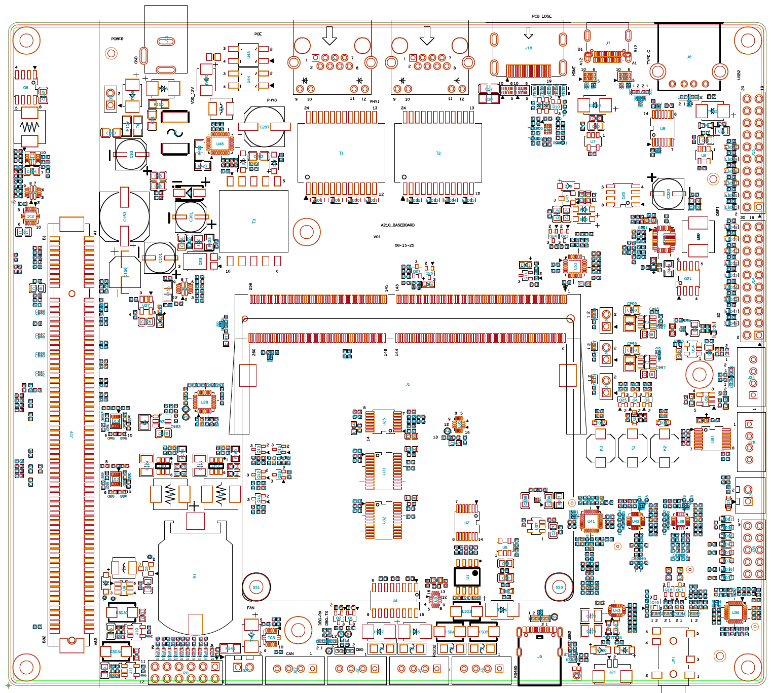
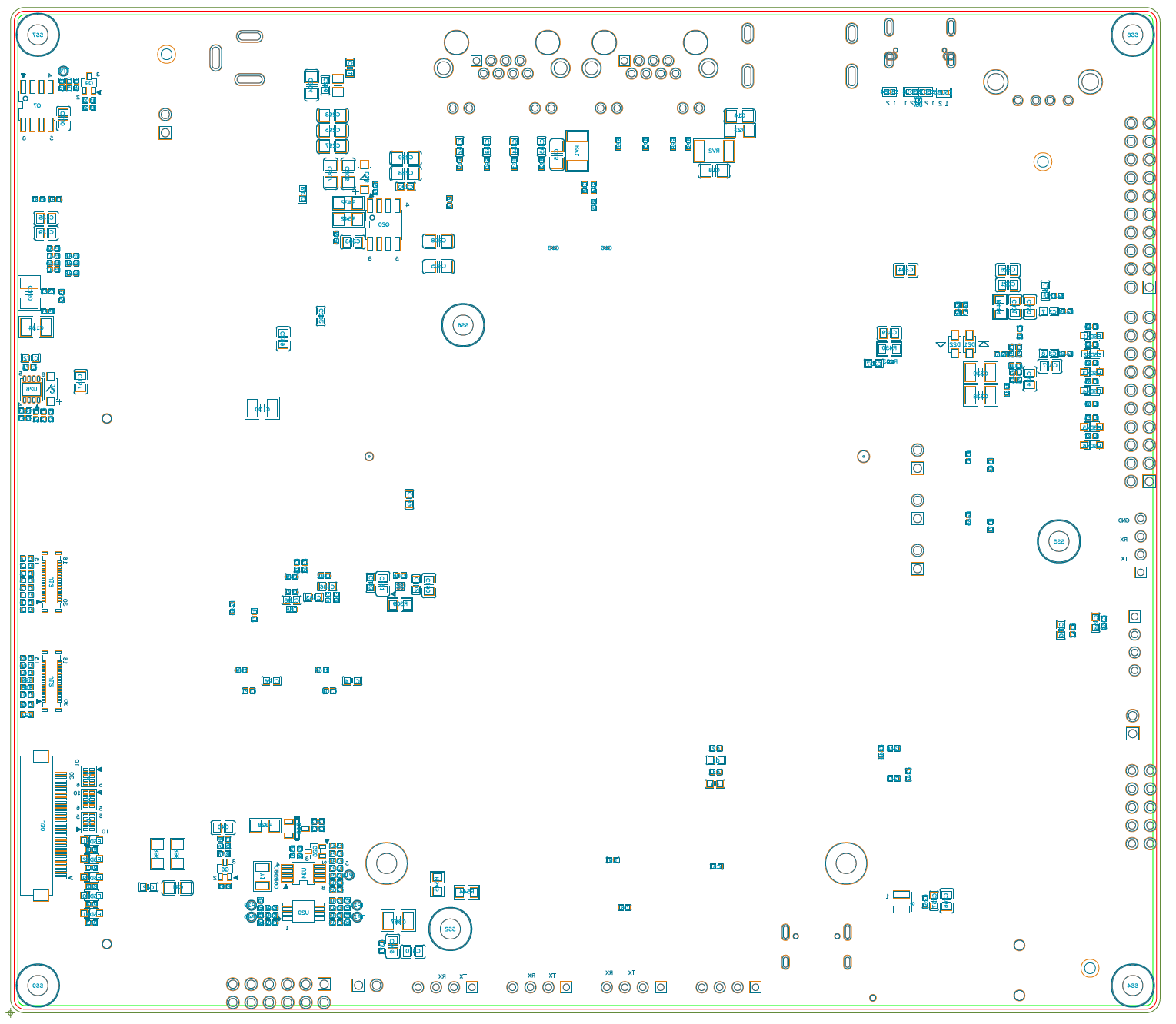
RefDes Diagram
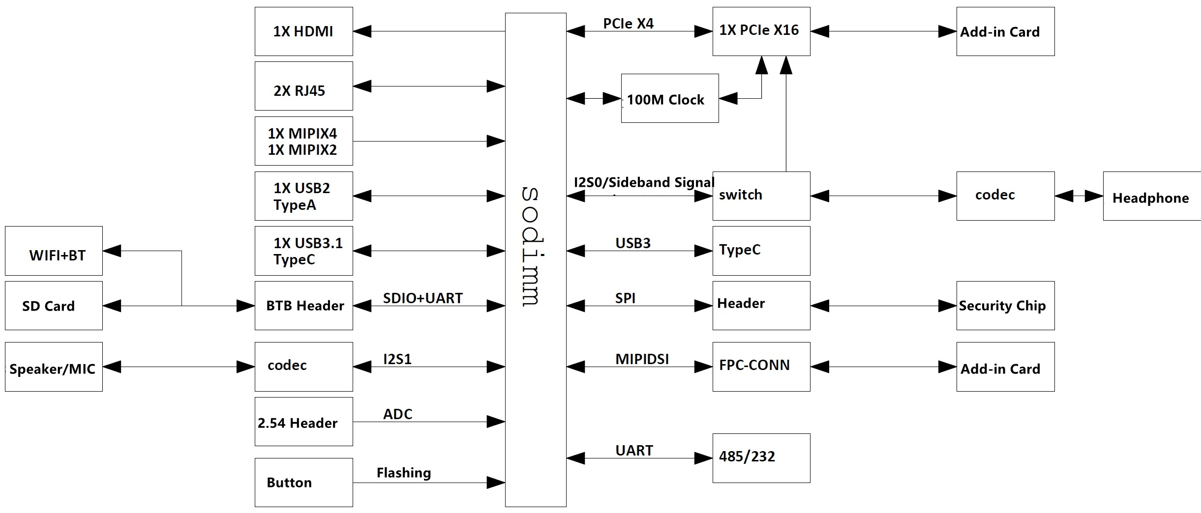
System Block Diagram
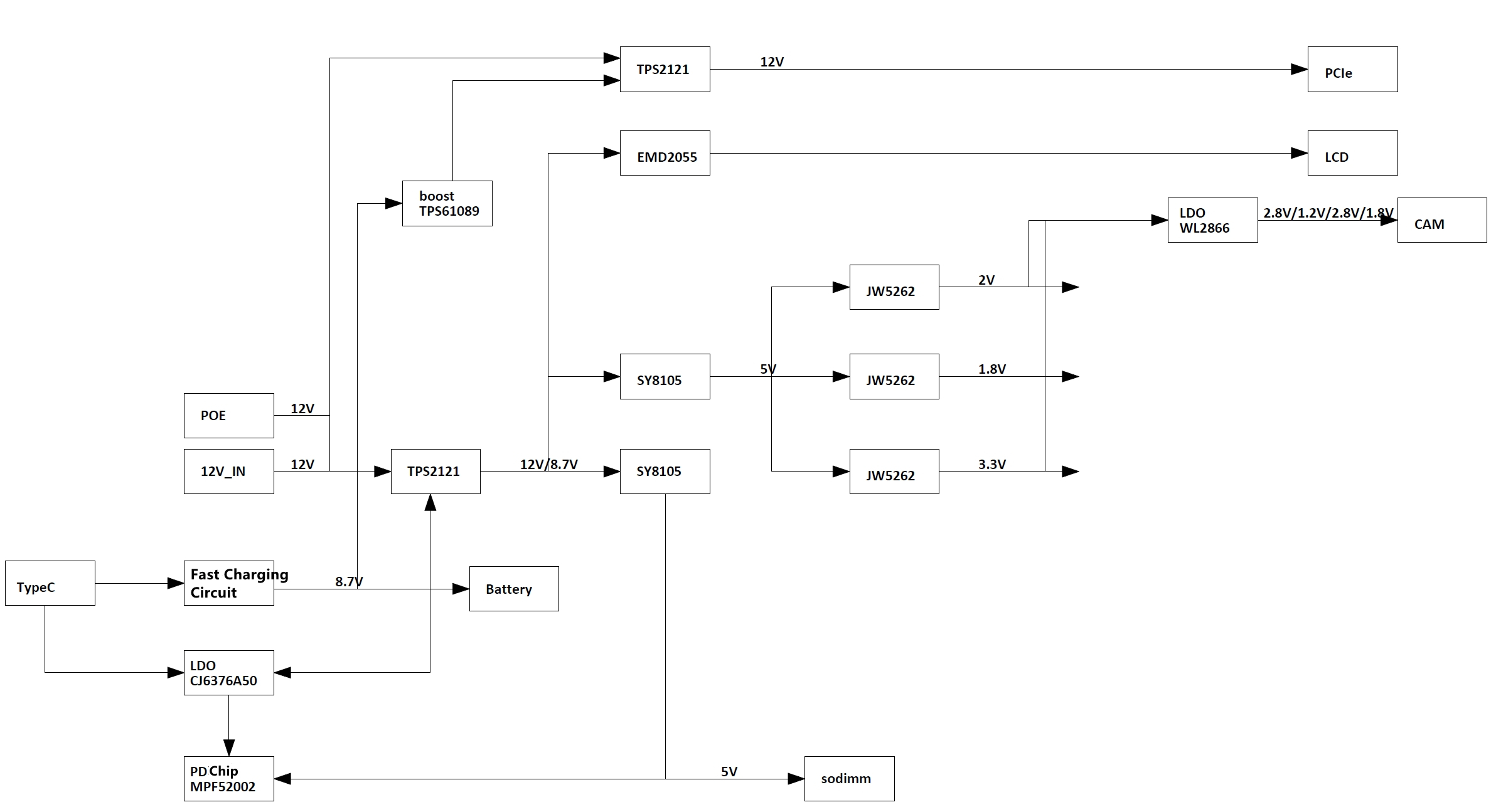
Power Block Diagram
Precautions and Configurations
The baseboard is designed for laboratory or engineering environments. Before starting operations, please read the following precautions:
Precautions
- Hot-plugging of the baseboard is not permitted under any conditions.
- To prevent electrostatic discharge (ESD) from damaging the base board hardware, take necessary anti-static measures before unpacking the board packaging and during installation.
- When handling the base board, hold it by the edges and avoid touching exposed metal parts to prevent static electricity from damaging the components.
- Please place the base board on a dry and flat surface, away from heat sources, electromagnetic interference sources, radiation sources, and electromagnetic radiation-sensitive devices (e.g., medical equipment).
Base Board Configurations
- The baseboard configures the operating modes of the A210 through pull-up/pull-down resistors.
- For boot mode settings, see BOOT_SEL Configuration.
- For PCIe RC/EP switching, see PCIe Mode Configuration.
- The baseboard supports POE, but only on RJ45 port #2. Comlipant with 802.3af/at protocols. Delivers up to 30W.
- The baseboard features a PCIe 3.0 x4 interface with bifurcation support. For the PCIe mode, see PCIe Mode Configuration.
- UART4 is the debug console for the A210 and is not recommended for other purposes.