A210 SODIMM V2 Baseboard
The A210 SODIMM V2 baseboard establishes the foundation for a basic development kit by connecting to a PC via serial port, USB, and Ethernet. To build a more comprehensive development or demo environment, you will need the following additional components:
- A display.
- An audio source and speakers
- USB 2.0/3.0 devices
- Storage media, such as a USB flash drive or a microSD (TF) card.
Features
A210 SODIMM V2 includes the following features.
- One 2x10 pin 2.54mm header provides expansion for a QSPI interface.
- One 2x10 pin 2.54mm header provides expansion for a UART interface.
- Two RJ45 Ethernet ports supporting 10/100/1000 Mbps in full-/half-duplex mode.
- One full-featured USB 3.1 port with DP ALT mode support.
- One USB 2.0 Type-A port for flashing.
- One USB 2.0 Type-A port.
- One Mini PCIe port supporting PCIe and USB.
- One M2-B SATA port.
- One HDMI 2.0 port.
- Analog audio input and output ports.
- One MIPI-DSI expansion port
- One 2-lane MIPI-CSI Board-to-Board (B2B) connector.
- One 4-lane MIPI-CSI Board-to-Board (B2B) connector.
- Integrated Wi-Fi and Bluetooth V5.0 /4.2 support.
Hardware Introduction
Connectors
A210 SODIMM V2 reserves a wealth of peripheral connectors.


The description of A210 SODIMM V2 connector is as follows.
| NO. | Description |
|---|---|
| 1 | Debug UART header |
| 2 | PCIe RC/EP mode switch |
| 3 | 5V fan header |
| 4 | HDMI connector |
| 5 | USB 3.1 TypeC connector with DP support |
| 6 | 3.5mm audio jack |
| 7 | Power button |
| 8 | sodimm socket |
| 9 | 12V DC Input |
| 10 | USB 2.0 Type A connector for flashing |
| 11 | USB 2.0 Type A connector |
| 12 | RJ45 connector |
| 13 | RJ45 connector |
| 14 | UART&GPIO header |
| 15 | SPI&GPIO header |
| 16 | Reset button |
| 17 | Flash button |
| 18 | MIPI CSI1 X2 FPC expansion Connector |
| 19 | MIPI CSI0 X4 Board-to-Board (B2B) expansion connector |
| 20 | MIPI DSI expansion connector |
| 21 | M2.B SATA connector |
| 22 | Mini PCIe slot |
QSPI0 Expansion Header
The baseboard provides a QSPI0 interface. Users can design and verify based on this header's pinout to connect an external QSPI Flash or TPM device.
- 2.54mm pin pitch header.
- Signal Logic Level: 1.8V.
- Power pins: 3V3(1.7A max current), 1V8(1.5A max current), VDD_5V(2A max current).
| pin net | pin | pin | pin net |
|---|---|---|---|
| VDD_5V | 1 | 2 | QSPI0_D3_HOLD |
| VDD_3V3 | 3 | 4 | QSPI0_SCLK |
| VDD_1V8 | 5 | 6 | QSPI0_D1_MISO |
| I2C7_SCL | 7 | 8 | QSPI0_D2_WP |
| I2C7_SDA | 9 | 10 | QSPI0_D0_MOSI |
| GND | 11 | 12 | QSPI0_CSN0 |
| GND | 13 | 14 | GPIO0_1 |
| GND | 15 | 16 | GPIO1_16 |
| GND | 17 | 18 | GPIO0_24 |
| GND | 19 | 20 | ADC_VIN_CH1 |
UART&GPIO Expansion Header
- 2.54mm pin pitch header.
- Signal Logic Level: 1.8V.
- Power pins: 3V3(1.7A max current), 1V8(1.5A max current), VDD_5V(2A max current).
| pin net | pin | pin | pin net |
|---|---|---|---|
| VDD_5V | 1 | 2 | UART8_CTSN |
| VDD_3V3 | 3 | 4 | UART8_RTSN |
| DD_1V8 | 5 | 6 | UART8_TXD |
| GPIO0_31 | 7 | 8 | UART8_RXD |
| GPIO0_28 | 9 | 10 | GPIO2_17 |
| GPIO1_1 | 11 | 12 | AOGPIO1_1 |
| GND | 13 | 14 | GPIO2_7 |
| GND | 15 | 16 | GPIO2_16 |
| GND | 17 | 18 | GPIO0_26 |
| GND | 19 | 20 | GPIO0_15 |
A210 Debug UART Header
- Type: XH2.54-4P.
- Power pins: 3V3.
| pin | pin_net |
|---|---|
| 1 | NC |
| 2 | TX |
| 3 | RX |
| 4 | GND |
MIPI DSI Expansion Connector
- Type: Flexible Printed Circuit (FPC) connector.
- An adapter board can be used for screen validation.
- Pins labeled for TP can also be repurposed for other functions.
- Power Rails: 3V3_TP (3.3V supply with 1.5A current limit), 3V3_D (3.3V supply with 1.5A current limit).
- LED_K/A: Backlight Power, up to 36V, 100 mA.
| pin | pin_net |
|---|---|
| 1 | 3V3_TP |
| 2 | TP_I2C_SDA |
| 3 | TP_I2C_SCL |
| 4 | TP_RST |
| 5 | TS_INT |
| 6 | GND |
| 7 | DISP_RST |
| 8 | GND |
| 9 | 3V3_D |
| 10 | 3V3_D |
| 11 | GND |
| 12 | MIPI_DSI0_DAT2N |
| 13 | MIPI_DSI0_DAT2P |
| 14 | GND |
| 15 | MIPI_DSI0_DAT1P |
| 16 | MIPI_DSI0_DAT1N |
| 17 | GND |
| 18 | MIPI_DSI0_CLKP |
| 19 | MIPI_DSI0_CLKN |
| 20 | GND |
| 21 | MIPI_DSI0_DAT0N |
| 22 | MIPI_DSI0_DAT0P |
| 23 | GND |
| 24 | MIPI_DSI0_DAT3N |
| 25 | MIPI_DSI0_DAT3P |
| 26 | GND |
| 27 | LED_K |
| 28 | LED_K |
| 29 | LED_A |
| 30 | LED_A |
MIPI CSI1 X4 FPC Expansion Connector
The baseboard provides a 4-lane MIPI-CSI interface.
- Power Management:
- Controlled by PMIC (WL2866) with adjustable voltage and current limiting.
- 2.8V_AVDD/1.8V_AVDD with 300mA max each, 1.2V_DVDD/1.8V_DVDD with 820mA max. each.
- Type: AFC01-S24FCA-00.
- Validating other camera modules requires an interposer board for signal bridging.
| pin | pin net |
|---|---|
| 1 | +2.8V |
| 2 | +1.2V |
| 3 | +1.8V |
| 4 | MIPI_CSI0_MCLK |
| 5 | GND |
| 6 | MIPI_CSI0_A_CLK_P |
| 7 | MIPI_CSI0_A_CLK_N |
| 8 | GND |
| 9 | MIPI_CSI0_B_DAT1_P |
| 10 | MIPI_CSI0_B_DAT1_N |
| 11 | MIPI_CSI0_B_DAT0_P |
| 12 | MIPI_CSI0_B_DAT0_N |
| 13 | MIPI_CSI0_A_DAT1_P |
| 14 | MIPI_CSI0_A_DAT1_N |
| 15 | MIPI_CSI0_A_DAT0_P |
| 16 | MIPI_CSI0_A_DAT0_N |
| 17 | GND |
| 18 | GND |
| 19 | MIPICSI0_SCL |
| 20 | MIPICSI0_SDA |
| 21 | CSI0_RST |
| 22 | CSI0_PWDN |
| 23 | NC |
| 24 | NC |
MIPI CSI1 X2 FPC Expansion Connector
The baseboard provides a 2-lane MIPI-CSI interface.
- Power Management:
- Controlled by PMIC (WL2866) with adjustable voltage and current limiting.
- 2.8V_AVDD/1.8V_AVDD with 300mA max each, 1.2V_DVDD/1.8V_DVDD with 820mA max. each.
- Type: AFC01-S24FCA-00.
- Validating other camera modules requires an interposer board for signal bridging.
| pin | pin net |
|---|---|
| 1 | NC |
| 2 | +2.8V |
| 3 | GND |
| 4 | MIPICSI1_SDA |
| 5 | MIPICSI1_SCL |
| 6 | GND |
| 7 | CSI1_RST |
| 8 | CSI1_PWDN |
| 9 | GND |
| 10 | MIPI_CSI1_MCLK |
| 11 | GND |
| 12 | MIPI_CSI1_A_CLK_P |
| 13 | MIPI_CSI1_A_CLK_N |
| 14 | GND |
| 15 | MIPI_CSI1_A_DAT0_P |
| 16 | MIPI_CSI1_A_DAT0_N |
| 17 | GND |
| 18 | MIPI_CSI1_A_DAT1_P |
| 19 | MIPI_CSI1_A_DAT1_N |
| 20 | GND |
| 21 | 1.8V |
| 22 | GND |
| 23 | 1.2V |
| 24 | GND |
M2.B SATA Connector
| pin net | pin | pin | pin net |
|---|---|---|---|
| NC | 1 | 2 | VDD_3V3 |
| GND | 3 | 4 | VDD_3V3 |
| GND | 5 | 6 | NC |
| NC | 7 | 8 | NC |
| NC | 9 | 10 | M2_SATA_EN |
| GND | 11 | ||
| NC | 21 | 20 | NC |
| NC | 23 | 22 | NC |
| NC | 25 | 24 | NC |
| GND | 27 | 26 | NC |
| NC | 29 | 28 | NC |
| NC | 31 | 30 | NC |
| GND | 33 | 32 | NC |
| NC | 35 | 34 | NC |
| NC | 37 | 36 | NC |
| GND | 39 | 38 | NC |
| PCIE_SLOT0_RX2_P | 41 | 40 | NC |
| PCIE_SLOT0_RX2_N | 43 | 42 | NC |
| GND | 45 | 44 | NC |
| PCIE_SLOT0_TX2_N | 47 | 46 | NC |
| PCIE_SLOT0_TX2_P | 49 | 48 | NC |
| GND | 51 | 50 | NC |
| NC | 53 | 52 | NC |
| NC | 55 | 54 | NC |
| GND | 57 | 56 | NC |
| NC | 59 | 58 | NC |
| NC | 61 | 60 | NC |
| NC | 63 | 62 | NC |
| NC | 65 | 64 | NC |
| NC | 67 | 66 | NC |
| NC | 69 | 68 | NC |
| GND | 71 | 70 | VDD_3V3 |
| GND | 73 | 72 | VDD_3V3 |
| NC | 75 | 74 | VDD_3V3 |
MINI PCIe Slot
The Mini PCIe slot, with support for PCIe and USB 2.0 protocols.
| pin net | pin | pin | pin net |
|---|---|---|---|
| MINPCIE_WAKE | 1 | 2 | VDD_3V3 |
| NC | 3 | 4 | GND |
| NC | 5 | 6 | VDD_1V5 |
| MINPCIE_CLKREQ | 7 | 8 | NC |
| GND | 9 | 10 | NC |
| REFCLK+ | 11 | 12 | NC |
| REFCLK- | 13 | 14 | NC |
| GND | 15 | 16 | NC |
| NC | 17 | 18 | GND |
| NC | 19 | 20 | NC |
| GND | 21 | 22 | MINPCIE_PERST |
| PCIE_SLOT0_RX1_N | 23 | 24 | VDD_3V3 |
| PCIE_SLOT0_RX1_P | 25 | 26 | GND |
| GND | 27 | 28 | VDD_1V5 |
| GND | 29 | 30 | NC |
| PCIE_SLOT0_TX1_N | 31 | 32 | NC |
| PCIE_SLOT0_TX1_P | 33 | 34 | GND |
| GND | 35 | 36 | USB2_PCIE_D1N |
| NC | 37 | 38 | USB2_PCIE_D1P |
| NC | 39 | 40 | GND |
| NC | 41 | 42 | NC |
| NC | 43 | 44 | NC |
| NC | 45 | 46 | NC |
| NC | 47 | 48 | VDD_1V5 |
| NC | 49 | 50 | GND |
| NC | 51 | 52 | VDD_3V3 |
WIFI &BT Module
WIFI Module: O-Net (Fn-Link) 6222B-SRC, RTL8822CS-VS-CG, Wi-Fi 802.11 a/b/g/n/ac, Wi-Fi+BT5.0, 2T2R, SDIO+UART.
Modules Introduction
BOOT_SEL Configuration
| Pin | Baseboard GPIO Pin | Function | Baseboard Configuration |
|---|---|---|---|
| BOOT_SEL0/AOGPIO0_1 | BOOT_SEL0 | Boot Mode Select | R65 Pull-up, R70 NC |
| BOOT_SEL1/AOGPIO0_2 | BOOT_SEL1 | Boot Mode Select | R64 NC, R69 Pull-down |
| BOOT_SEL2/AOGPIO0_23 | BOOT_SEL2 | Boot Mode Select | R494 NC, R495 Pull-down |
Boot Mode Settings
| ID | BOOT_SEL2 | BOOT_SEL1 | BOOT_SEL0 | Boot Mode Setting |
|---|---|---|---|---|
| 0 | 0 | 0 | 0 | CCTBoot/USB Download |
| 1 | 0 | 0 | 1 | eMMC Boot(baseboard default) |
| 2 | 0 | 1 | 0 | SPI NOR Boot, QSPI1, CS0 |
| 3 | 0 | 1 | 1 | SPI NAND Boot, QSPI1, CS0 |
| 4 | 1 | 0 | 0 | Forced CCTBoot |
| 5 | 1 | 0 | 1 | SD Boot, SDIO0 |
| 6 | 1 | 1 | 0 | SPI NOR Boot, QSPI0, CS0 |
| 7 | 1 | 1 | 1 | SPI NAND Boot, QSPI0, CS0 |
Note: If you need to change the boot mode, modifications must be made by soldering.
PCIe Mode Configuration
| Pin | Baseboard GPIO Pin | Function | Baseboard Configuration |
|---|---|---|---|
| AOGPIO1_8/PCIe_RC_EP_SEL | PCIe_RC_EP_SEL | PCIe Mode Select | J29 1: RC mode, pin left floating. 0: EP mode, shunted with jumper cap. |
The baseboard supports a PCIe 3.0 x4 interface with lane bifurcation capability. The available configurations are as follows:
| PHY | PHY0(x2) | PHY1(x2) | ||
| lane# | 0 | 1 | 2 | 3 |
| NO. | Configuration | |||
| 1 | X4 | |||
| 2 | X2 | X1 | ||
| 3 | X2 | SATA | SATA | |
| 4 | X1 | X1 | SATA | SATA |
- SOC integrates 2 PCIe controllers and 2 SATA controllers.
- PCIe Controllers: supports PCIE3.0 protocol.
- PHY0 Controllers: supports PCIe in both RC and EP modes. Lane configurations: X4, X2, X1.
- PHY1 Controllers: supports RC mode only. Lane configurations: X1 only.
- SATA Controllers: supports SATA3.0 protocol.
- The baseboard is equipped with a M2.B SATA connector and a Mini PCIE slot.
I2C Address Assignment
The chips used at the board level are shown in the figure below.
Note: Ensure there are no I2C address conflicts when adding devices via reserved interfaces.
| I2C BUS | Device | I2C Address |
|---|---|---|
| AOI2C | AW9523 | 0100000 |
| AW9523 | 0100001 | |
| FUSB302BMPX | 0100010 | |
| TP | 0010100/1011101 | |
| I2C4 | RTC | 1010001 |
| I2C5 | aud0_ADC | 1000000 |
| AUD0_DAC | 0001000 | |
| I2C6 | 4line sensor | —— |
| sensor PWR | 0101000 | |
| I2C7 | 2line sensor | —— |
| sensor PWR | 0101000 |
Power Control Description
| Pin | Controller | Net Name | Description |
|---|---|---|---|
| AOGPIO0_29 | A210 | POWER_5V_EN | VDD_5V enable signal. 1: enable, 0: disable. |
| AOGPIO0_26 | A210 | POWER_3V3_EN | VDD_3V3 enable signal. 1: enable, 0: disable. |
| GPIO0_30 | A210 | FAN_PWR_EN | FAN power enable signal. 1: enable, 0: disable. |
| P06 | AW9535-1 | PCIE_ETH_3V3_PWREN | PCIE Ethernet port 3.3V power enable. 1: Enable, 0: Disable. |
| GPIO0_27 | A210 | USB_TypeC_PWREN | USB3.1 Type-C power enable signal. 1: enable, 0: disable. |
| P16 | AW9535-1 | MIPI_DSI_PWREN | MIPI_DSI power enable signal. 1: enable, 0: disable. |
| P05 | AW9535-1 | MIPI_TP_PWREN | MIPI_TP power enable signal. 1: enable, 0: disable. |
| P17 | AW9535-1 | BL_EN | Display backlight power enable. 1: enable, 0: disable. |
| GPIO2_12 | GPIO2_12 | PWM1_CH2 | Backlight brightness control (PWM). |
| P04 | AW9535-1 | MIPI_CSI1_PWREN | MIPI power enable signal. 1: enable, 0: disable. |
| P03 | AW9535-1 | MIPI_CSI0_PWREN | MIPI power enable signal. 1: enable, 0: disable. |
| P13 | AW9535-1 | SDIO_3V3_PWREN | Wi-Fi module 3.3V power enable signal. 1: enable, 0: disable. |
| P14 | AW9535-1 | SDIO_1V8_PWREN | Wi-Fi module 1.8V power enable signal. 1: enable, 0: disable. |
| P06 | AW9535-0 | MINPCIE_1V5POWER_EN | Mini PCIe 1.5V power enable signal. 1: enable, 0: disable. |
| P07 | AW9535-0 | MINPCIE_3V3_PWREN | Mini PCIe 3.3V power enable signal. 1: enable, 0: disable. |
| P16 | AW9535-0 | M2_SATA_3V3_PWREN | SATA 3.3V power enable signal. 1: enable, 0: disable. |
| P15 | AW9535-1 | PI6C557_PWREN | PCIe clock generator power enable signal. 1: enable, 0: disable. |
| P10 | AW9535-1 | USBCON_PWREN | USB 2.0 power enable signal. 1: enable, 0: disable. |
| P11 | AW9535-1 | USBCON1_PWREN | USB power enable signal(active when port acts as a host during programming). 1: enable, 0: disable. |
| P01 | AW9535-1 | AUDIO_3V3_PWREN | Audio ADC/DAC 3.3V power enable signal. 1: enable, 0: disable. |
| P02 | AW9535-1 | AUDIO_1V8_PWREN | Audio ADC/DAC 1.8V power enable signal. 1: enable, 0: disable. |
General-purpose GPIO Signal Description
| Pin | Controller | Net Name | Description |
|---|---|---|---|
| GPIO2_0 | A210 | UART4_TXD | UART signal. |
| GPIO2_1 | A210 | UART4_RXD | UART signal. |
| P00 | AW9535-1 | PCIE_ETH_PERSTB | PCIE_ETH reset signal (active low). |
| AOGPIO1_7 | A210 | TYPEC_DPTX_AUX_PUPDCTL1 | Pull-up/pull-down control signal for the AUX channel when the Type-C interface carries DP signals. |
| AOGPIO0_30 | A210 | TYPEC_DPTX_AUX_PUPDCTL2 | Pull-up/pull-down control signal for the AUX channel when the Type-C interface carries DP signals. |
| AOGPIO0_28 | A210 | USBCC_INT_L | Type-C CC (Configuration Channel) interrupt (active low). |
| AOGPIO0_27 | A210 | RTC_INT | RTC chip interrupt (active low). |
| GPIO3_4 | A210 | TP_RST | TP reset (active low). |
| AOGPIO1_0 | A210 | TS_INT | TP interrupt (active low). |
| P15 | AW9535-0 | DISP_RST | MIPI DSI display reset (active low). |
| P01 | AW9535-0 | CSI1_RST | MIPI_CSI reset (active low). |
| P00 | AW9535-0 | CSI1_PWDN | MIPI_CSI sensor power-down (active low). |
| P04 | AW9535-0 | CSI0_RST | MIPI_CSI reset (active low). |
| P03 | AW9535-0 | CSI0_PWDN | MIPI_CSI sensor power-down (active low). |
| GPIO3_0 | A210 | MIPI_CSI0_MCLK | MCLK for the sensor. |
| GPIO3_1 | A210 | MIPI_CSI1_MCLK | MCLK for the sensor. |
| GPIO0_14 | A210 | WL_EN | Wi-Fi module enable signal. |
| AOGPIO1_3 | A210 | WL_WAKE_HOST | Wi-Fi module wake-up signal to the host. |
| AOGPIO0_30 | A210 | BT_WAKE_HOST | BT module wake-up signal to the host. |
| GPIO0_17 | A210 | HOST_WAKE_BT | Host wake-up signal to the BT module. |
| AOGPIO1_3 | A210 | BT_EN | BT module enable signal. |
| GPIO3_10 | A210 | UART5_RTSN | UART signal used for Bluetooth control. |
| GPIO3_9 | A210 | UART5_CTSN | UART signal used for Bluetooth control. |
| GPIO2_18 | A210 | UART5_TXD | UART signal used for Bluetooth control. |
| GPIO2_19 | A210 | UART5_RXD | UART signal used for Bluetooth control. |
| AOGPIO1_5 | A210 | MINPCIE_WAKE | Mini PCIe wake-up signal. |
| P17 | AW9535-0 | MINPCIE_PERST | Mini PCIe reset signal. |
| GPIO0_25 | A210 | PCIE_X1_CLKREQ_N | Mini PCIe clock request. |
| P11 | AW9535-0 | M2_SATA_EN | SATA enable signal. |
| P14 | AW9535-0 | PI6C557_EN | PCIe clock generator enable signal. |
| P12 | AW9535-0 | AUDIO_ADC0_INT | Audio ADC interrupt. |
| ADC IN CH0 | A210 | ADC_VIN_CH0 | Headphone mic input. |
| P13 | AW9535-0 | HP_CTL_H | Headphone output enable. |
| GPIO0_16 | A210 | HP_DET_L | Headphone insertion detection. |
| GPIO2_5 | I2S1_DOUT | Audio I2S signal. | |
| GPIO2_4 | I2S1_DIN | Audio I2S signal. | |
| GPIO2_3 | I2S1_LRCK | Audio I2S signal. | |
| GPIO2_2 | I2S1_BCLK | Audio I2S signal. | |
| GPIO2_6 | I2S1_MCLK | Audio I2S signal. |
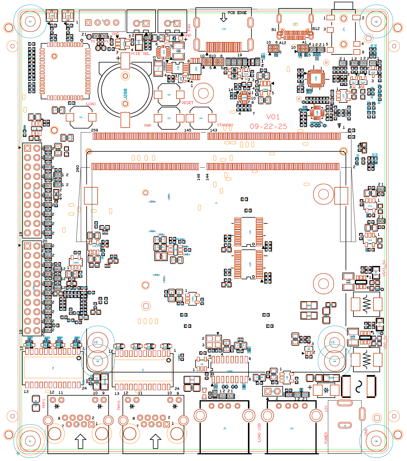
RefDes Diagram

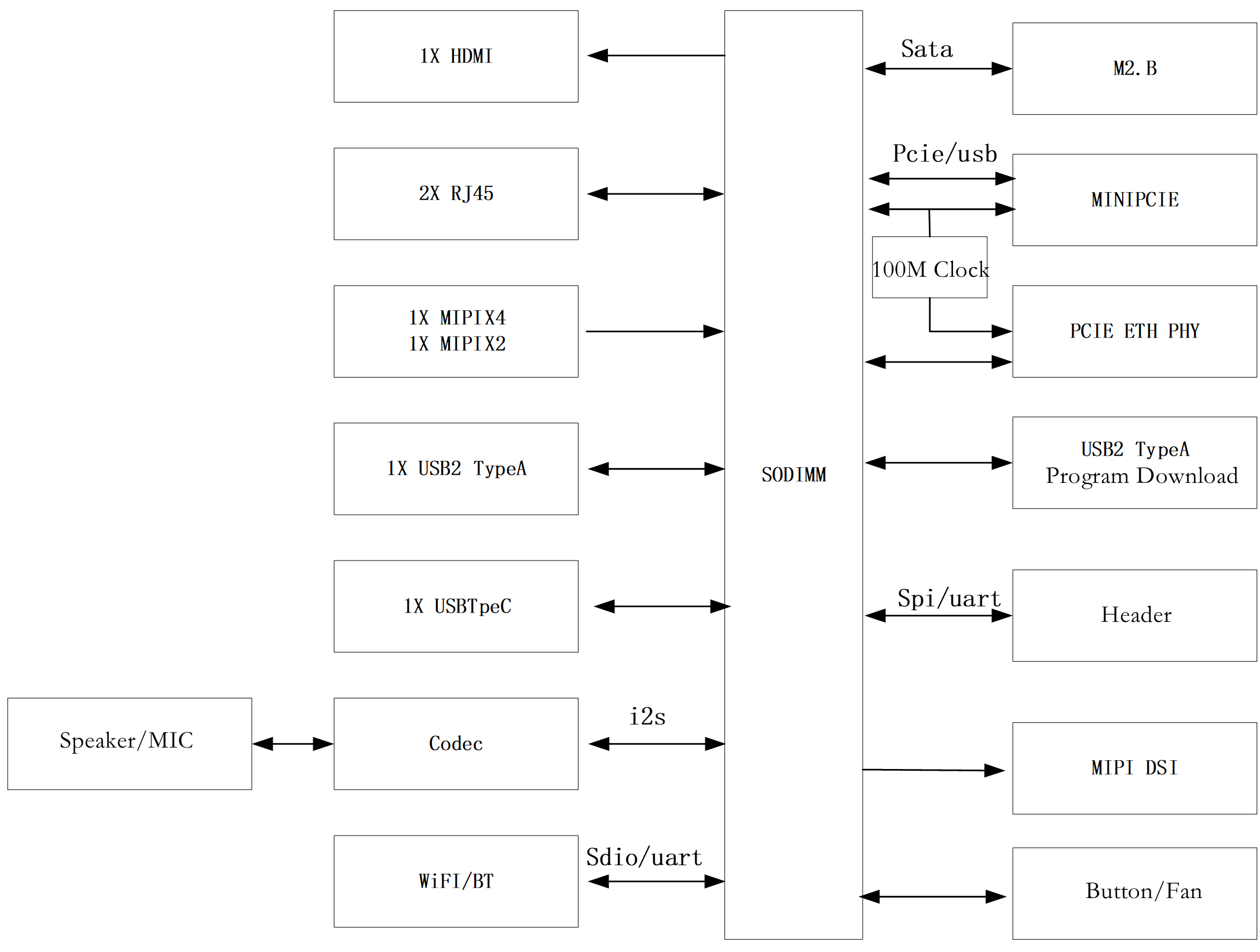
System Block Diagram
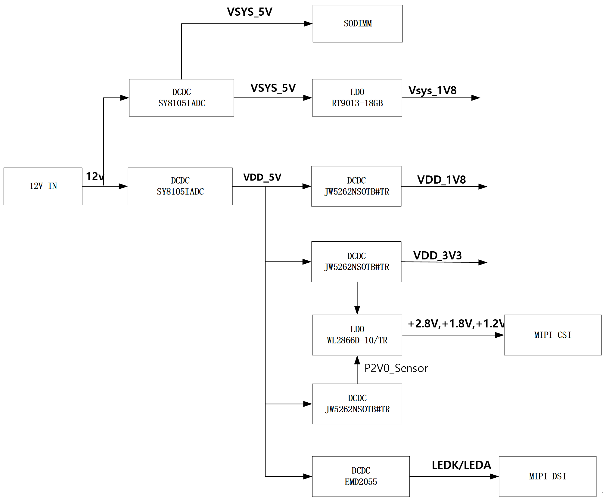
Power Block Diagram
Precautions and Configurations
The baseboard is designed for laboratory or engineering environments. Before starting operations, please read the following precautions:
Precautions
- Hot-plugging of the baseboard is not permitted under any conditions.
- To prevent electrostatic discharge (ESD) from damaging the base board hardware, take necessary anti-static measures before unpacking the board packaging and during installation.
- When handling the base board, hold it by the edges and avoid touching exposed metal parts to prevent static electricity from damaging the components.
- Please place the base board on a dry and flat surface, away from heat sources, electromagnetic interference sources, radiation sources, and electromagnetic radiation-sensitive devices (e.g., medical equipment).
Baseboard Configurations
- The baseboard configures the operating modes of the A210 through pull-up/pull-down resistors.
- For boot mode settings, see BOOT_SEL Configuration.
- For PCIe RC/EP switching, see PCIe Mode Configuration.
- UART4 is the debug console for the A210 and is not recommended for other purposes.