PCB Design Recommendations
PCB Stackup Design
To minimize reflections during high-speed signal transmission, impedance matching must be done between the signal source, receiver, and transmission lines.
The specific impedance of a single-ended signal line depends on its trace width and the relative position to the reference plane. The trace width/spacing for differential pairs with specific impedance requirements depends on the chosen PCB stackup structure. Since the minimum trace width and spacing depend on the PCB type and cost requirements, the selected PCB stackup structure must meet all impedance requirements on the board, including inner and outer layers, single-ended and differential lines, etc.
Design principles for layer definition.
- Ideally, a symmetric structure design should be adopted. Symmetry includes the thickness and type of dielectric layers, copper foil thickness, and symmetry of the distribution of graphics (power layers, signal layers).
- The adjacent layers to the main chip should be complete ground planes, providing reference planes for device surface routing.
- The main power supply should be adjacent to its corresponding ground plane layer as much as possible.
- All signal layers should be adjacent to ground planes, and direct adjacency between two signal layers should be avoided as much as possible to provide a complete reference ground plane.
- If adjacent routing between two layers is required, the distance between them should be as far as possible, and the signals should be oriented perpendicular to each other to minimize inter-layer signal crosstalk.
Recommended PCB layer definition scheme: When determining the specific PCB layer configuration, the above principles should be flexibly applied based on actual requirements. Avoid rigidly following a predefined layout.
Currently, A210-1DIE-FCBGA mainly employs 8-layer through-hole vias and 10-layer 3rd-order blind/buried vias (designed for C2C routing) for the stackup. The following stackup is provided as an example to assist engineers in selecting and evaluating stackup structures. If choosing a different type of stackup, please recalculate the impedance based on the specifications provided by the PCB manufacturer.
8-Layer PCB Stackup
In the design of an 8-layer PCB stackup, it is recommended to stack the layers as follows: TOP-Gnd-Signal-GND-Power/Signal--Power/Signal-Gnd-Bottom. The reference plane for the top signal layer (L1) is L2, and the reference plane for the bottom signal layer (L8) is L7. The signal layers L3 have reference planes L2 and L4, with L2 being the primary reference plane. The specific configuration may vary depending on the stackup requirements. The copper thickness for all layers should be 1oz. The diagram below shows a reference stackup for a 1.6mm board thickness, and the core thickness can be adjusted based on the board thickness requirements.
10-Layer 3rd-Order Stackup
It is recommended to adopt a 10-Layer 3rd-Order Stackup and route the C2C signals between the L2 and the L4 layers to meet the requirement of C2C interconnect quality. The internal layer routing effectively achieves low crosstalk. The blind and buried vias are essential to eliminate via stubs. It is recommended to stack the layers as follows: TOP-GND/Signal-Signal-Signal/GND–POWER-POWER- GND-Signal/POWER-GND-Bottom. The reference plane for the top signal layer (L1) is L2, and the reference plane for the bottom signal layer (L10) is L9. The signal layers L2 have reference planes L1 and L3. The signal layers L4 have reference planes L3 and L5. The specific configuration may vary depending on the stackup requirements. The diagram below shows a reference stackup for a 1.6mm board thickness, and the core thickness can be adjusted based on the board thickness requirements.
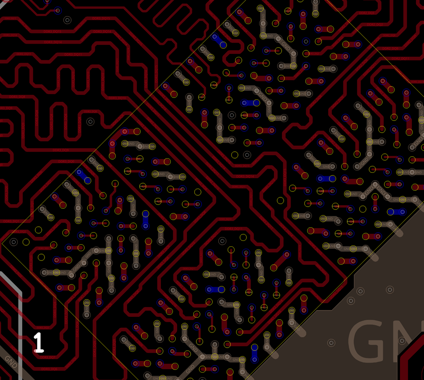
Fanout Design for A210-1DIE-FCBGA
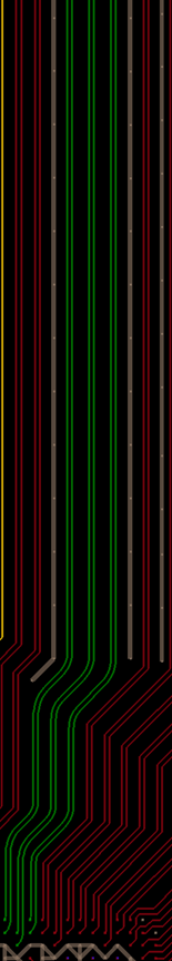
The A210-FCBGA package has a total of 1373 balls, with a 0.6mm pitch, as shown in the diagram below.
-
Outer two circles of Ball's fan-out design
For the A210-1DIE-FCBGA SoC, the fanout design should of the outermost two rows of balls and some of the balls in the third row, from the TOP layer, routing can be done with a minimum trace width of 4mil for local fanout. After that, it is recommended to transition to the corresponding characteristic impedance traces as soon as possible, with the minimum trace width kept short, following the required line width and spacing for fanout.
-
The inner rows of ball's fan-out design
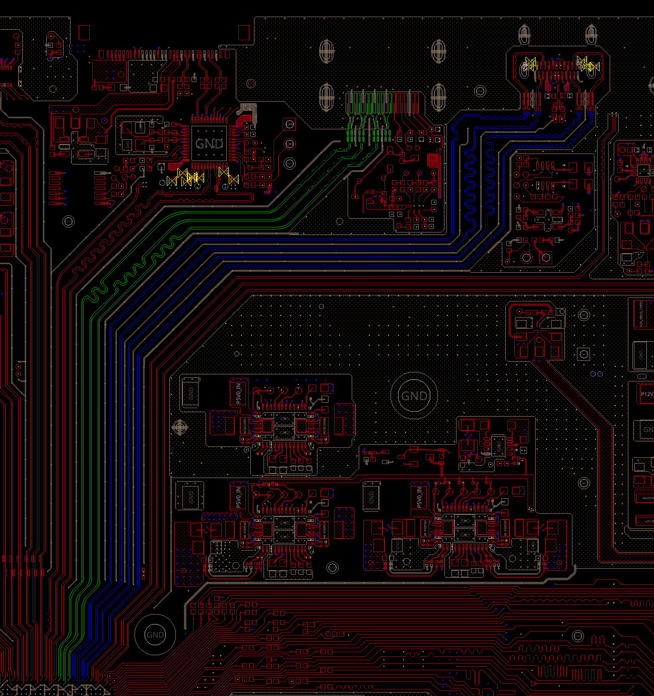
Starting from the third row, it is necessary to transition to inner layers. The transition vias should be placed in a regular pattern, and it is recommended to have a gap of 2-4 rows between each transition via row, allowing for larger channels for the ground and power planes.
In the case of the ground plane copper cladding pictured below, there are multiple channels connected to the outside ground, which facilitates signal integrity, power integrity as well as heat dissipation.
The power plane should have regular placement of vias to provide as large a copper coverage as possible for various power supplies, improving power delivery quality.
After the regular placement of vias, the routing can use a 3.5mil trace width for fanout.
General Layout Recommendations
Suggestions for Allegro
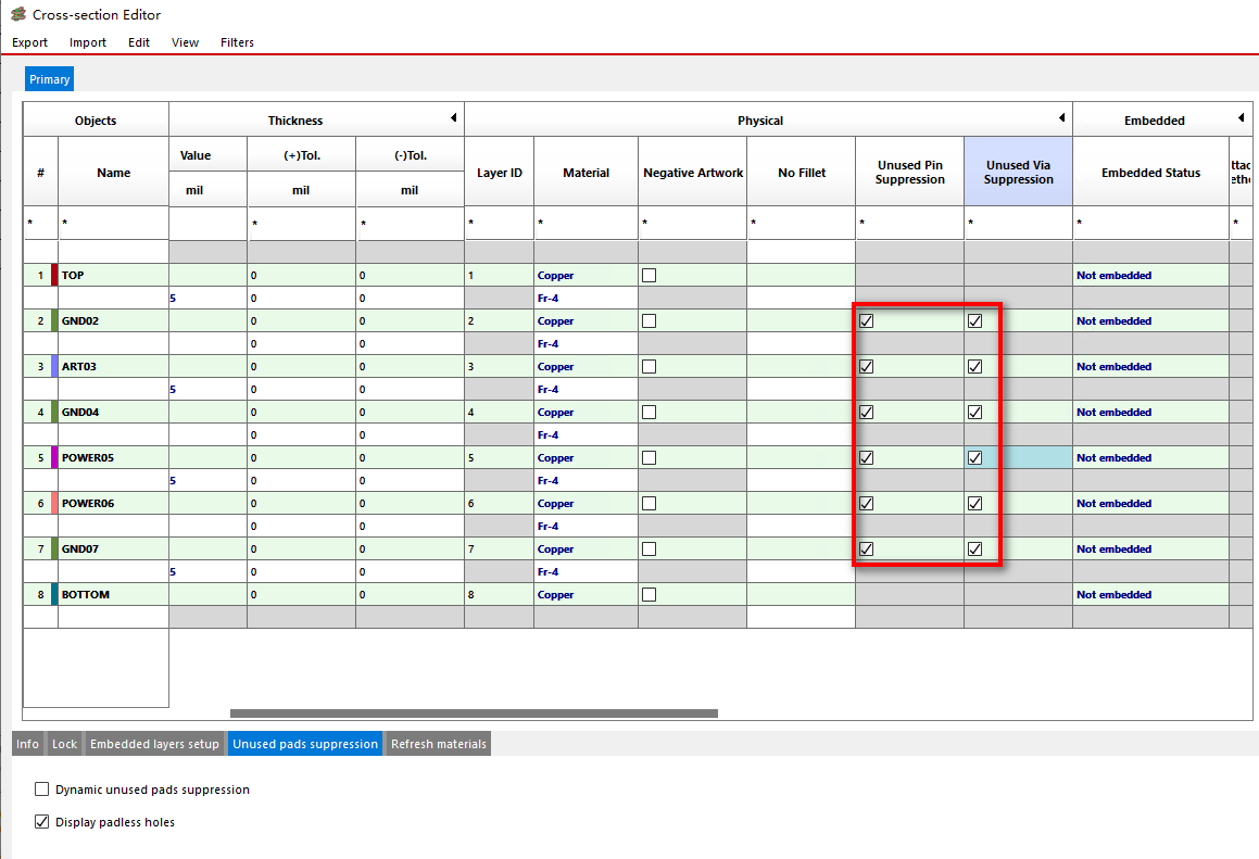
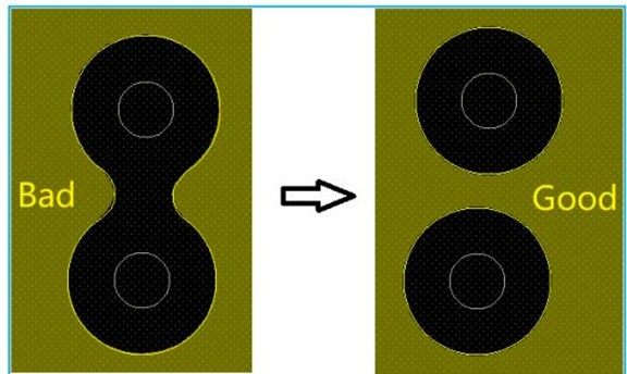
Non-functional annular rings can damage the copper plating and increase parasitic capacitance of vias. It is recommended to remove non-functional annular rings and solder rings on inner layers to enhance the integrity of copper planes. In Allegro, you can disable non-functional annular rings and solder rings on inner layers using the following methods:
Select allegro 17.4 version:Xsection-Physical-Unused Pads/Via Suppression, Check the pins and vias you want to disable.
Layout Recommendations
-
Interface Placement: Unless limited by structural constraints or length-matching requirements, place the interfaces as close as possible to the main A210-1DIE-FCBGA chip. Keep the overall trace lengths as short as possible, especially for critical signal lines.
-
Component Placement: Consider debugging, maintenance, and heat dissipation when arranging components.
-
Circuit Module Layout: Aim for balanced, compact, and aesthetically pleasing layouts for circuit modules, while minimizing loop areas.
-
Spacing between Circuit Modules: Provide appropriate spacing between different circuit modules to reduce mutual interference, especially for high-frequency components.
-
Decoupling Capacitor Placement: Place decoupling capacitors as close as possible to the power pins of the IC to minimize the loop formed between power and ground.
-
Clock Signal Termination Resistors: Place the series termination resistors for clock signals, such as eMMC clock, close to the A210-1DIE-FCBGA (SoC) side.
-
Place the series connected resistors for TX signals close to the transmitting end and for RX signals close to the receiving end. Keep the trace lengths between the pins and resistors within 400mil.
For example, for GMAC's TXD0-TXD3, TXCTL, and TCLK, place the series matching resistors close to the A210-1DIE-FCBGA (source) end, and for RXD0-RXD3, RXCTL, and RXC, place the series matching resistors close to the PHY end.
The placement of GMAC series resistors is shown in the figure below.
The placement of GMAC RX series resistors is shown in the figure below.
-
Place ESD protection components near the interfaces, and consider placing coupling capacitors near connectors.
The placement of ESD protection components is shown in the figure below.
The placement of coupling capacitors is shown in the figure below.
Routing Recommendations
-
Trace length should include package and via.
-
Minimize sharp corners in routing, and consider using 135-degree angles instead of 90-degree angles.
-
Remove all non-functional pads.
-
Avoid routing around clock devices (such as crystals, oscillators, clock buffers), switching power supplies, magnetic components, and through-holes for connectors.
-
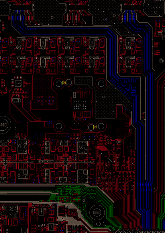
It is recommended to reserve sufficient spacing for high-speed SERDES signals, Specifically, TX and RX pairs should be isolated grounded or separated by a sufficient distance.
The isolated grounding for USB3 TX and RX trace routing is shown in the figure below.
-
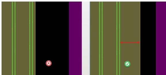
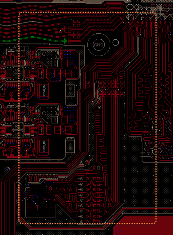
Avoid crossing different regions with high-speed signals. It is recommended to keep a distance of at least 40mil between the high-speed signal and the edge of the reference plane. The high-speed signal and reference plane edge is shown in the figure below.
-
Use serpentine routing to reduce crosstalk caused by routing.
-
Minimize the stub length as much as possible, it is recommended to keep the stub length as zero. The trace stub is shown in the figure below.
-
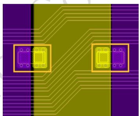
Due to reduced impedance caused by surface-mounted component pads, to minimize the impact of impedance variation, it is recommended to remove a layer of the reference plane directly below the pad. Common surface-mounted components include capacitors, ESD protection devices, common mode chokes, connectors, etc. The removal of reference plane under surface-mounted component pads is shown in the figure below.
-
When copper is placed on the connector pads, ensure that the ground copper does not exceed the ground pad. The copper placement on connector pads is shown in the figure below.
-
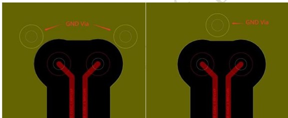
It is recommended to have at least one ground via near each ground pad of a high-speed connector, and the via should be placed as close as possible to the pad. The ground via near connector pad is shown in the figure below.
-
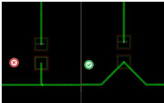
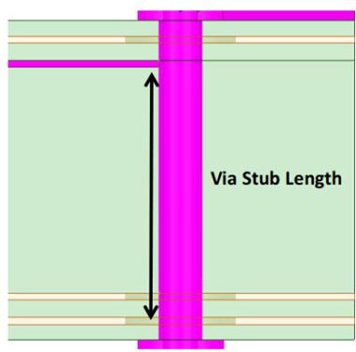
Avoid the stub effect of vias, especially when the stub length exceeds 12mil. It is recommended to evaluate the impact of via stubs on signal integrity through simulation. The via stub effect is shown in the figure below.
-
It is recommended to have one ground via for each GND pin of ICs (such as eMMC chips, flash chips). The ground via for IC GND pins is shown in the figure below.
-
It is recommended to have one ground via for each GND pin of ESD protection devices, and the via should be placed as close as possible to the pad. The ESD device with ground via is shown in the figure below.
-
When changing layers and the reference planes before and after the change are ground planes, place a companion via next to the signal via to ensure the continuity of the return path. For single-ended signals, it is recommended to place a return via next to the signal via to reduce crosstalk between vias. The single-ended signal via transition is shown in the figure below.
-
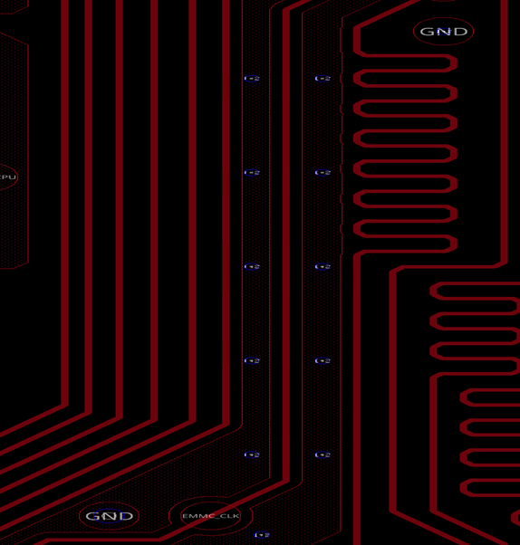
For important high-speed single-ended signals such as clock signals, reset signals (e.g., emmc_clk, emmc_datastrobe, RGMII_CLK, etc.), it is recommended to surround them with ground traces. Place a ground via every 500mil along the ground trace. The ground trace for single-ended signals is shown in the figure below.
-
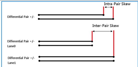
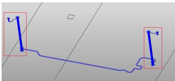
Intra-pair skew is the term used to define the difference length between + and - in a differential pair. Inter-pair skew is used to define the difference length between a differential pair and another differential pair. The space between signals is defined as air-gap distance. The differential pair skew is shown in the figure below.
-
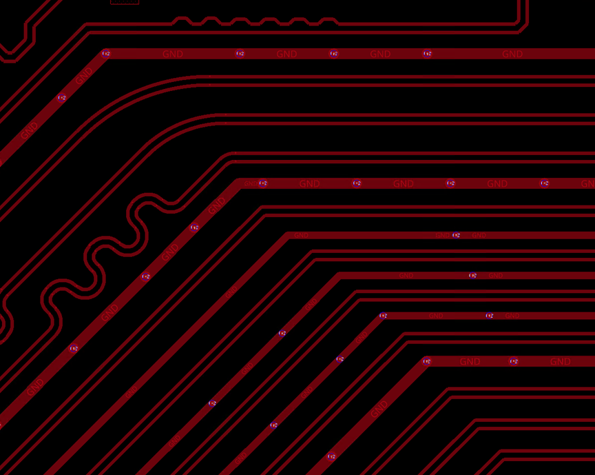
Route trace over continuous GND plane without interruption. Any discontinuity or split on the reference plane will degrade signal integrity significantly. The incomplete reference plan is shown in the figure below.
-
When the reference plane of the routing has cross-power layers, it is recommended that ground capacitance be added to each of the 2 power layers to provide a complete return path. The cross-power plan is shown in the figure below.
-
Differential signals require equal lengths within pairs, that is, the time delay difference between P and N should be as small as possible. Therefore, when the time delay difference occurs between the differential lines P and N, the nearby winding is compensated. Special attention should be paid to the size of the winding, which should meet the requirements shown in the figure below to reduce the impact of sudden changes in impedance. The winding dimension is shown in the figure below.
-
Place ground stitching vias near the signal transition vias. For differential signals, both signal vias and stitching vias should be placed symmetrically. The gnd via for differential via is shown in the figure below.
-
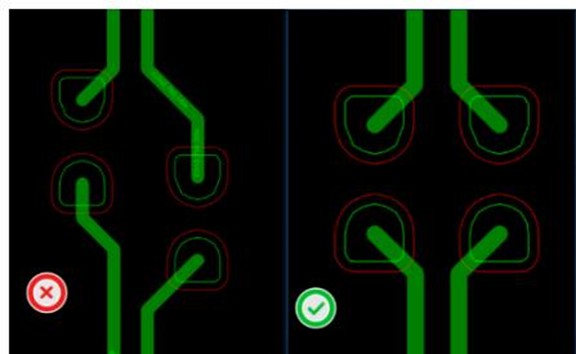
Route differential pairs on symmetry. The symmetry layout is shown in the figure below.
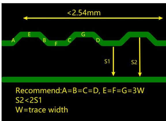
Routing Requirements for Signal Running ≥ 5GT/s
Some of the A210-1DIE-FCBGA interface signals can work in 5GT/s and above rate, due to the high rate, PCB design requirements will be more stringent, in the Layout Recommendations chapter based on the need to be in accordance with the requirements of this chapter to the wiring.
-
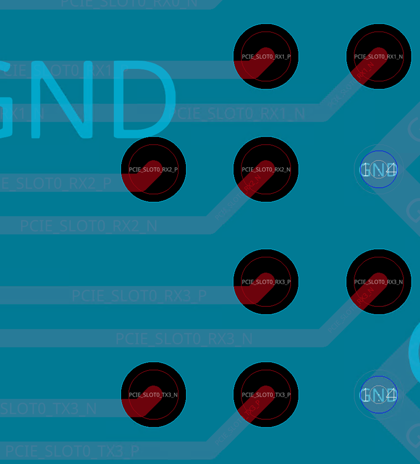
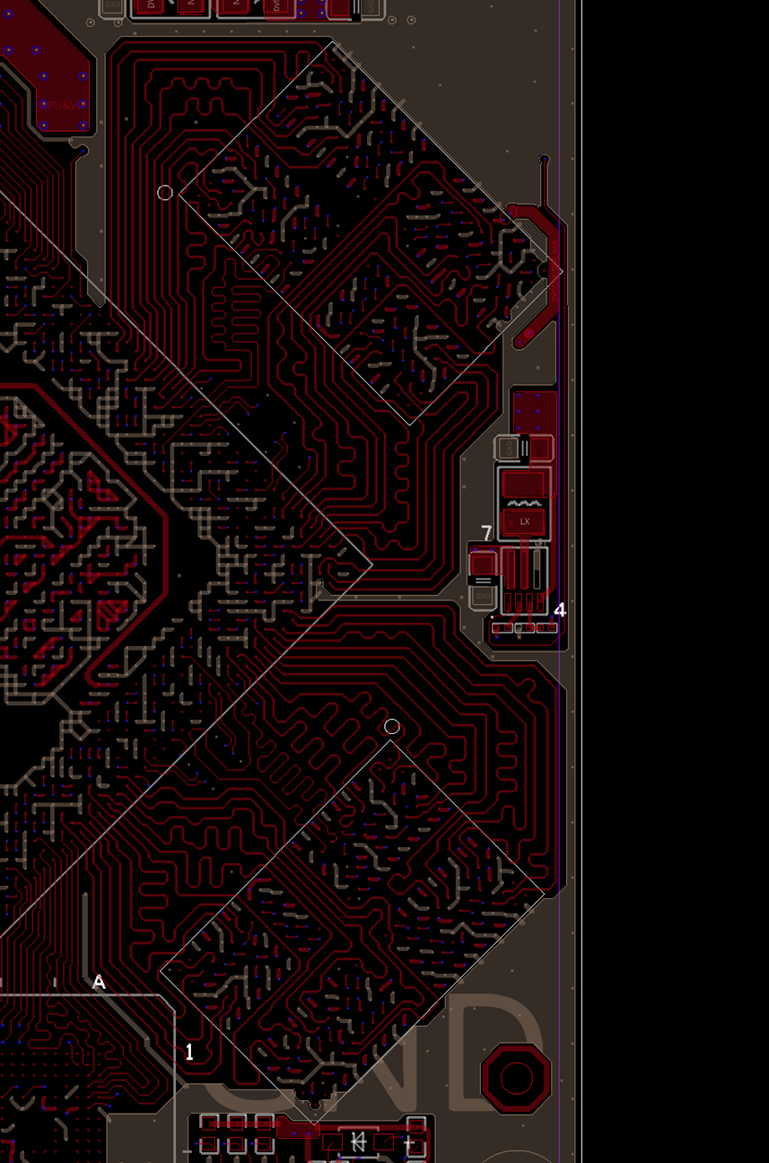
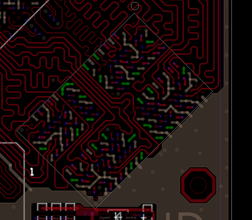
Void the Ground Plane Under the BGA Pads. It is recommended to void the L2 reference plane directly beneath the signal pads and use L3 as the reference layer instead to reduce capacitance and enhances impedance control. The voiding size is 7mil in radius. The reference plane voiding is shown in the figure below.
-
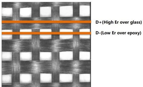
。Void the Ground Plane Under the BGA Pads. The glass weave effect refers to the difference in dielectric constant between the glass fiber and epoxy resin used to fill and laminate PCB substrates. When the D+ trace of a differential pair is located above the resin filling while the D- trace is located above the glass fiber, it can result in different characteristic impedances and time delays between the D+ and D- traces. This leads to a timing skew within the differential pair, which can affect the eye diagram quality. The glass weave effect is shown in the figure below.
When the data rate of the interface reaches 5GT/s and the trace length exceeds 2 inches, it is important to carefully address the glass weave effect. It is recommended to use the following methods to mitigate the impact of the glass weave effect.
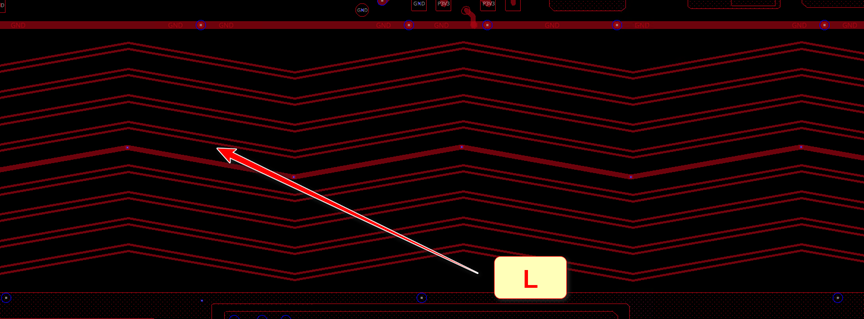
When the routing angle is 10°, the width "W" in the diagram should be at least 3 times the distance between glass weaves. The recommended values are W=60mil, θ=10°, L=340mil. Please notice that L should be at least exceed 240mil to span any possible glass weaves. The 10° routing angle is shown in the figure below.
Modules PCB Design Recommendations
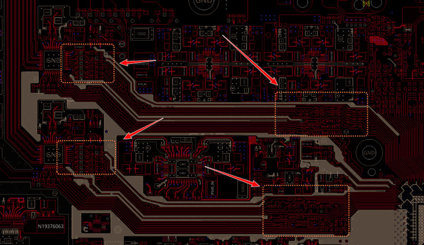
- When laying out the interfaces/functional modules, unless constrained by structural limitations or length matching requirements, it is advisable to place the interfaces as close to the A210-1DIE-FCBGA as possible, with short traces, minimal layer changes, and no crossings.
- It is recommended to replicate the layout and routing of the reference template provided by our company for the minimum system, which includes A210-1DIE-FCBGA, LPDDR4/4x, and PMIC.
- Without affecting the power plane, it is recommended to place as many back-drilled ground vias as possible in the various functional areas below the A210-1DIE-FCBGA (SoC).
- All signals of the interface circuits/functional modules should be grouped together and fully surrounded by a ground plane, isolated from signals of other modules to reduce mutual interference. The spacing between the back-drilled vias for ground connection should be ≤ 300mil. The reference layer for all signals should be a complete ground plane to avoid interrupted signal return paths caused by consecutive vias.
- When signals need to change layers, it is recommended to add back-drilled vias near the position within 30mil, and the two back-drilled vias for differential signals should be symmetrically placed.
- Decoupling capacitors for the corresponding power domain under the A210-1DIE-FCBGA (SoC) should be placed close to the corresponding power pins. Each capacitor should be paired with one or more power vias and ground vias. The power fan-out should be wide and quickly widened to 10mil or more.
- Decoupling capacitors for grain ends/interface circuits must be placed near the corresponding pins, with short and wide traces to meet their respective current requirements.
- Please refer to the Layout Recommendations and the specific recommendations for each interface below.
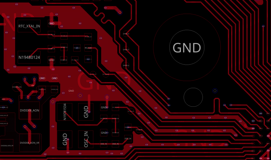
Clock Circuit PCB Design
In the PCB design of the clock circuit, please pay attention to the followings.
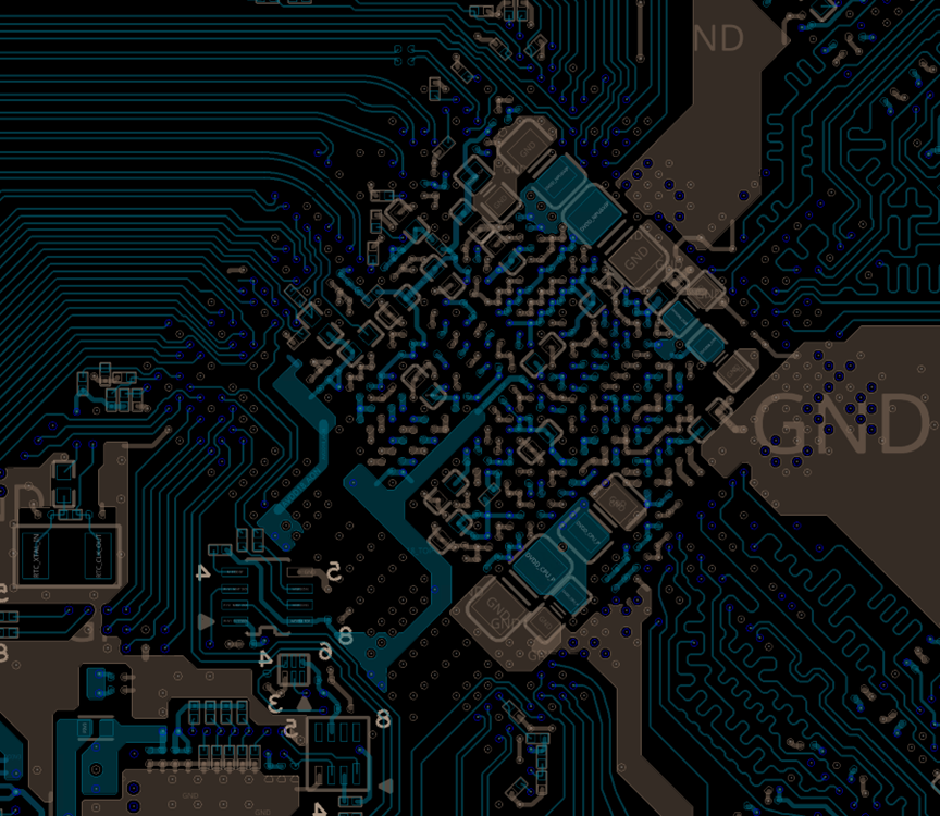
- The layout of the crystal circuit should be given priority. It should be placed on the same layer as the chip and as close as possible to avoid drilling vias. The traces of the crystal should be kept short, away from sources of interference, and preferably far from the board edges.
- The crystal and clock signals should be fully surrounded by a ground plane. Every 200-300mil, a GND via should be added to the ground trace, and the ground reference plane on the adjacent layer must be intact.
- If the crystal circuit is placed on a different layer than the chip, the crystal traces must be fully surrounded by a ground trace to avoid interference.
- No traces are allowed near the projection area below the crystal to prevent noise coupling into the clock circuit.
- On the top layer below the crystal, a ground ring can be placed. The ground ring is connected to the adjacent ground plane through vias to isolate noise.
- The second layer below the crystal should maintain an intact ground reference plane without any trace cuts to help isolate noise and maintain the crystal's output.
The crystal layout and traces for A210-1DIE-FCBGA is shown in the figure below.
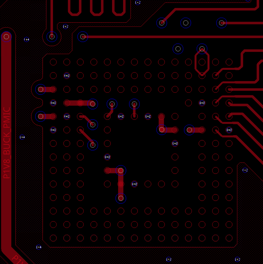
PMIC/Power Circuit PCB Design
PCB Design for ZH70809 Power Solution
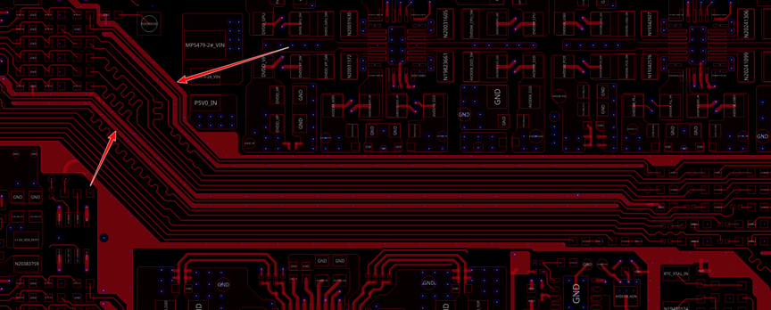
In the overall layout, from the perspective of power quality, ZH70809 should be placed as close to A210-1DIE-FCBGA as possible (considering heat dissipation design, it should be placed appropriately, not too close or too far). When placing it, prioritize arranging the traces (copper) from the power sources with higher output currents of ZH70809 to A210-1DIE-FCBGA in a continuous manner, avoiding crossing if possible.
Caution:
- The negative terminal of high-current BUCK input/output capacitors should have the same number of vias as the positive terminal to achieve better filtering effect (many engineers tend to overlook the vias for the negative terminal of capacitors), and it is recommended to connect the large GND copper foils together.
- It is not recommended to use "thermal pads" for the solder pads or holes of power components. They should be fully covered with copper. It is recommended to cover the copper on the power pins of ZH70809. All pins should be connected to the outside through traces, The width of the copper coverage should be the same as the width of the pins (should not exceed the width of the pins) to prevent solder bridging issues when the solder pads become larger during PCB fabrication.
The distribution of ZH70809 vias is shown in the figure below.

-
PCB Design Requirements for ZH70809 BUCK1-8
- For areas requiring vias, if VCC5V is combined for power supply, at least 2 vias with an inner diameter of 10Mils is needed. If they are separated, each should have at least 1 via with an inner diameter of 10Mils.
- Input capacitor requirements: The input capacitors must be placed as close to the chip as possible. If the input capacitors are placed on the backside of the chip, ensure that the connection loop between the input capacitors, VCC, and GND are minimized.
- SW trace requirements: The SW traces should be kept as short and wide as possible, and their copper area should be increased as much as possible to improve current capability and power efficiency.
- Power output via requirements: Determine the number of vias based on the actual application current.
The layout and traces for ZH70809 is shown in the figure below.
ZH70300 Circuit PCB Design
ZH70300 Fan-out adopts Via-in-Pad (VIP) design for fan-out, with a 6Mil drill (inner diameter) and a 12Mil pad (outer diameter). The ZH70300 PCB Fan out is shown in the figure below.
DC-DC Low Voltage High Current Power Supply Feedback Compensation Suggestions
In the A210-1DIE-FCBGA PMIC solution, for several high-current BUCK power supply sources, considering voltage, current, ripple, and PCB layout, two feedback compensation strategies are proposed.
-
Proximal Feedback
Place the output capacitor Cout near the DC/DC and connect the feedback sampling point (FB/VOUT) to the output filter capacitor Cout's unconnected end. The proximal feedback PCB layout is shown in the figure below.
-
Distal Feedback. The distal feedback PCB layout is shown in the figure below.
Power PDN and Capacitor Filtration Requirements
| Power | PDN Ztarget for PCB (2MHz~20MHz) |
|---|---|
| DDR VDDQ | VDDQ = 5%×1.1V/1.06A = 0.052 for SoC VDDQ = 5%×1.1V/2A = 0.025 for DRAM |
| DDR VDDQLP | VDDQLP = 3%×0.6V/0.7A = 0.026 for SOC ≥ 3%×0.6/1.4A = 0.013 for DRAM |
| AVDD08_MIPI (DVDD08_TOP) | Ztarget=5%×0.8V / 3.6A =0.011ohm |
| DVDD_DDR | Ztarget=5%×0.8V/2.3 = 0.017 |
| DVDD08_D2D | Ztarget =5%×0.8V/2.4A =0.016 |
| AVDD08_D2D | Ztarget =5%×0.8V/0.8A =0.05 |
| C908 | Ztarget =5%×1V/ 3.522A =0.014 |
| C920 | Ztarget =5%×1V/ 5.547A =0.009 |
| NPU_VIP | Ztarget =5%×1V/ 13.768A =0.0036 |
| NPU_SS | Ztarget =5%×1V/ 2.258A =0.022 |
| GPU | Ztarget =5%×0.8V/ 1.419A =0.028 |
| VP | Ztarget =5%×0.8V/ 1.2A =0.033 |
| DVDDM | Ztarget =5%×0.8V/0.3A = 0.133ohm 对 DVDDM |
| 0.8V peripheral digital/analog circuit supply | Ztarget= 5%×0.8V/0.4A = 0.1ohm |
| 1.8V | Ztarget=5%×1.8V/ 0.4A =0.225ohm |
| 3.3V and PLL | Ztarget=5%×3.3V / 0.1A =1.5ohm for 3.3V Ztarget= 5%×0.8V/0.1A = 4 ohm for PLL |
The reference configuration for vias and capacitors for high-current core power supply is as follows.
| A210-1Die-BGA capacitor reference board | |||
|---|---|---|---|
| Vias | 0201 Capacitors (placed on the PCB Bottom layer under the SoC) | Other Capacitors (placed as close to the SoC as possible, based on the package size) | |
| NPU_VIP | 12 Through-holes | 15 0201_1uF | 220uF+100uF+10uF |
| NPU_SS | 9 Through-holes | 6 0201_1uF | 10uF |
| C920(CPU_P) | 17 Through-holes | 10 0201_1uF | 10uF+22uF+100uF+220uF |
| GPU | 7 Through-holes | 6 0201_1uF | 10uF |
| VP | 6 Through-holes | 5 0201_1uF | 10uF |
Note:
- It is recommended to refer to the minimum system design and do not change the capacitor configuration. Always prioritize smaller package sizes.
- Ball 与 Capacitor。If the blind and buried vias are adopted, ensure they are placed as close to the BGA balls as possible to provide the shortest path between the Ball and the Capacitor.
- Please reserve as many vias as possible. However, ensure the via does not "perforate" the power planes.
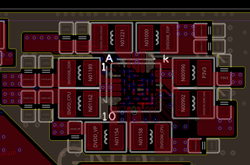
A210-1DIE-FCBGA Other LDO Power Supplies
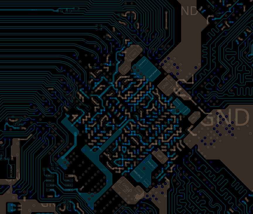
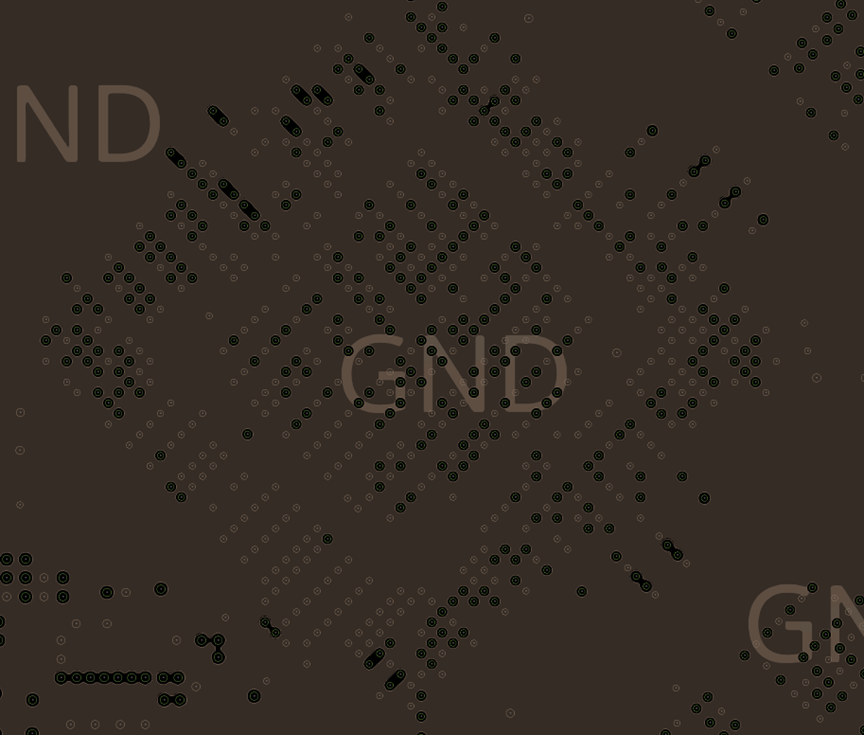
For other power supplies beneath the A210-1DIE-FCBGA(SoC), it is recommended to have one corresponding power via for each ball, if possible. Additionally, near the power vias and without affecting the power routing, it is advisable to add GND return vias. It is preferable to have a complete GND return plane on the adjacent layer of the power traces.
The decoupling capacitors for the other power supplies of the A210-1DIE-FCBGA should be placed close to the chip's pins. When using backside placement, the capacitors should be placed on the backside of the chip's pins. Ideally, the routing should pass through the capacitor pads before reaching the chip's pins. Each capacitor's GND pad should correspond to a dedicated GND via.
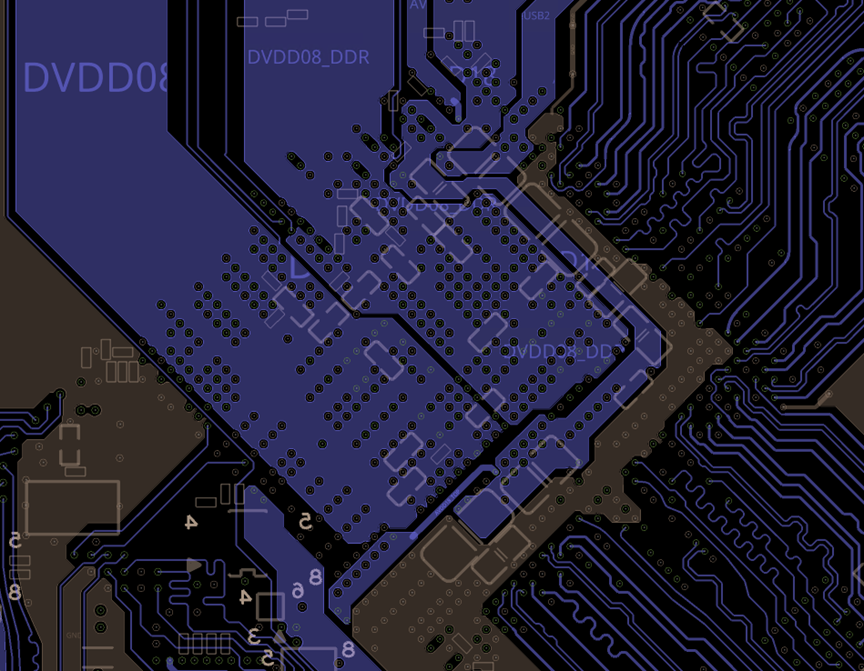
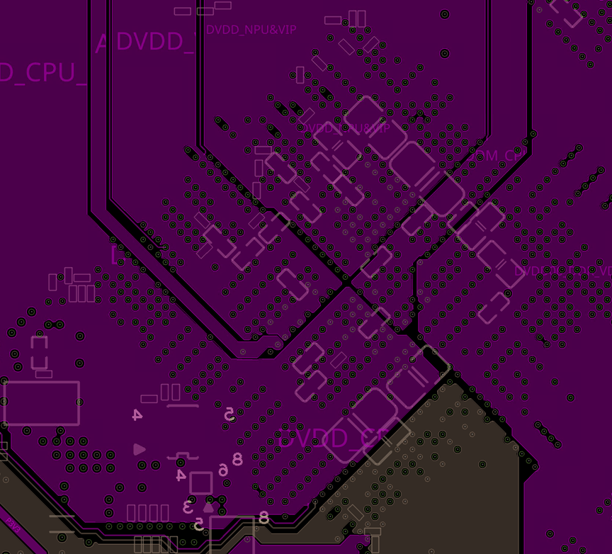
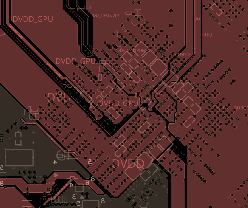
The A210-1DIE-FCBGA other power supply pin layout and vias is shown in the figure below.
The A210-1DIE-FCBGA other power supplies inner fan-out is shown in the figure below.
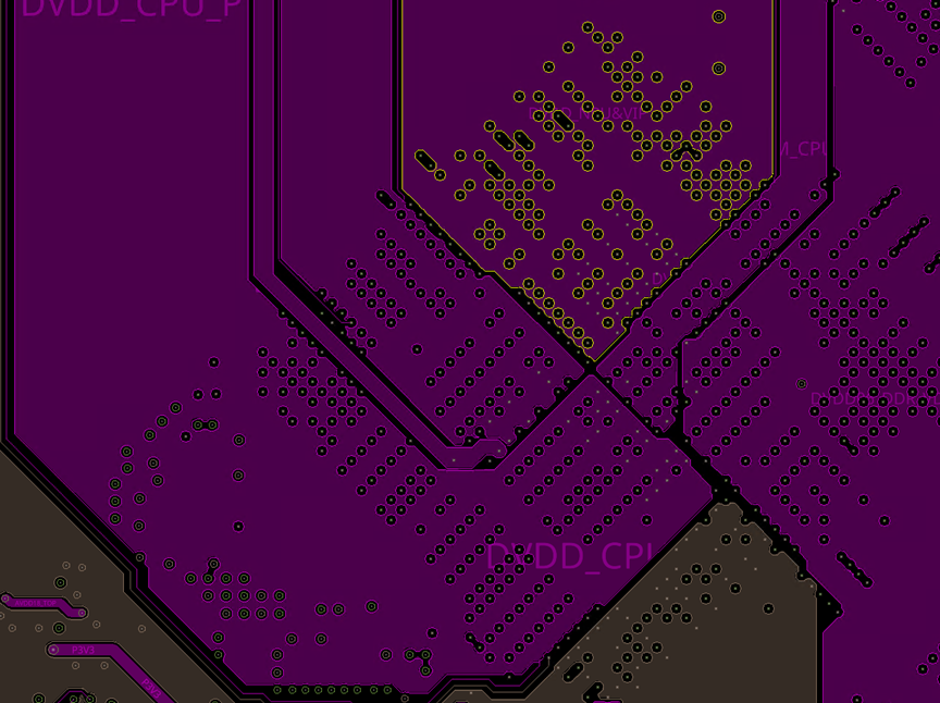
The decoupling capacitor on the back of the power supply pin of A210-1DIE-FCBGA other power supplies is shown in the figure below.
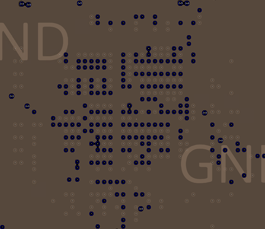
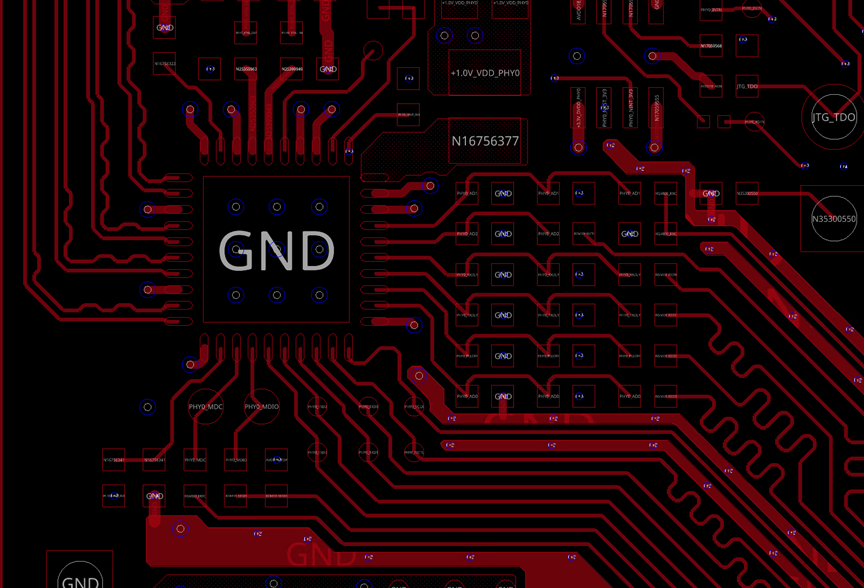
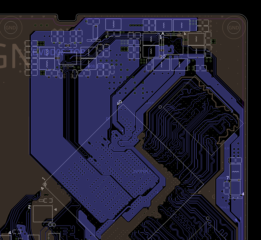
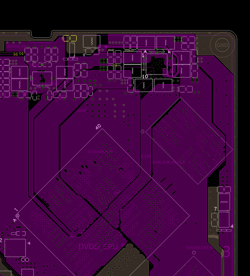
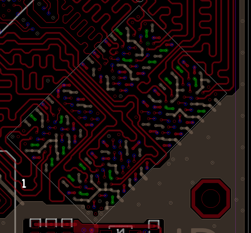
A210-1DIE-FCBGA VSS Pins
It is recommended to have as many GND return vias as possible for the VSS pins of the A210-1DIE-FCBGA(SoC) chip, without affecting the power plane. On the top layer, it is suggested to create a "#" pattern or densely populate traces in a crisscross manner. The recommended trace width is 10 mil.
The adjacent layers of the RK3576 (SoC) chip must form a complete GND plane, ensuring that the main reference ground is located near the CPU's ball. The ground vias should connect all VSS pins of the A210-1DIE-FCBGA(SoC) and the entire ground plane. This ensures power integrity, provides better Signal Integrity (SI) and Power Integrity (PI) conditions, and enhances PCB heat dissipation.
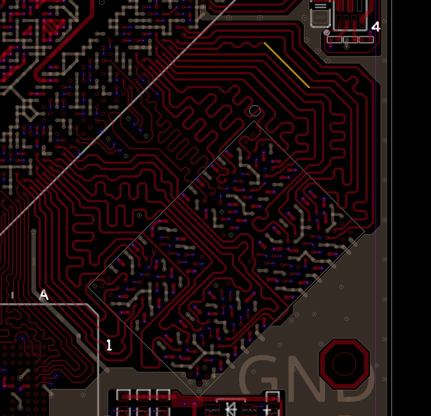
The distribution of BGA area vias and pads for A210-1DIE-FCBGA is shown in the figure below.
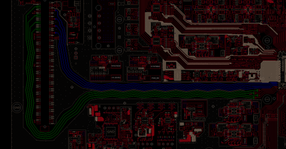
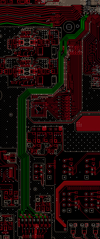
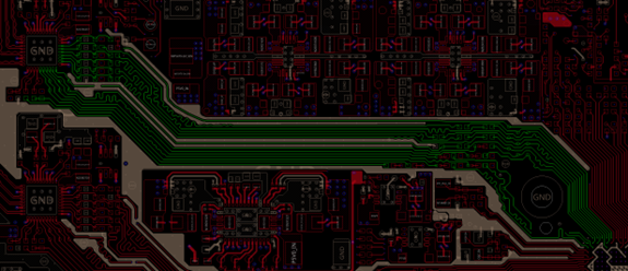
LPDDR4/4X PCB Design
As A210-1DIE-FCBGA LPDDR4/4X interface operates at 4266Mbps, the PCB design is difficult, so it is strongly recommended to use the DDR template provided by our company. If you do not use DDR templates and design PCB by yourself, please refer to the following PCB design suggestions, then perform time-domain eye diagram simulation and complete SI evaluation.
| Signal | Constraint | LPDDR4/4x |
|---|---|---|
| Electrical | Via Count | ≤2 vias per trace (including fanout area) |
| Propagation Delay (length for reference) | The trace is as short as possible. For DQ/DQS signals, 500mil~1000mil is properly. Do not exceed 2 inches. | |
| Static Phase (Intra-pair Skew) | DQS, CK: 5mil | |
| Relative Delay (Inter-pair/Group Skew) |
| |
| Physical | Impedance |
|
| Spacing | DQ | Based on simulation results. Requirement: PCB routing power-sum crosstalk must be < -40dB@0~2.1GHz. Pay extra attention to inter-group spacing; maintain at least 5H between groups. This is often overlooked in automated simulations. |
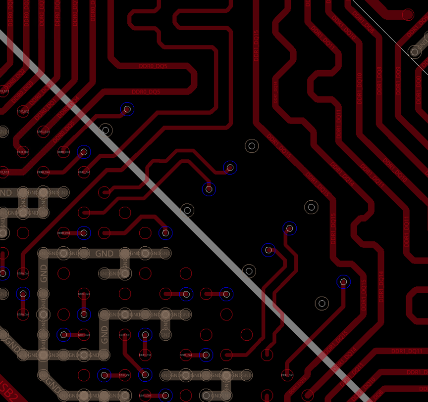
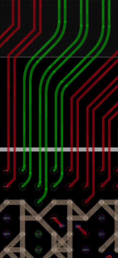
The vias design of 8-layer PCB LPDDR4/4X area is as follows.
-
If a signal trace changes layer and the reference plane is GND, stitching GND vias should be added close to the layer change vias within 25 mils. One Signal via should have ≧one GND via. Increase GND via as much as you can.
The schematic of the GND via corresponding to the signal via is shown in the figure below.
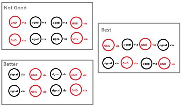
-
GND vias recommend to be placed between signal vias. Four signal vias together is not recommended. Use GND vias to separate signal vias as shown in the figure below, will improve performance.
The schematic of different via design is shown in the figure below.
-
For an 8-layer board, it is recommended to route DDR signals on the first layer, fourth layer, and sixth layer. The signals DQ, DQS, address and control signals, and CLK signal should have at least one complete GND reference plane. It is not recommended for the signals to refer to both the GND plane and the power plane at the same time, please refer to the ground plane entirely.
-
To avoid a break in the signal reference layer caused by a via, you can optimize the reference layer with GND traces. The GND traces optimization the reference layer is shown in the figure below.
-
The recommended distance between the trace and the edge of the reference layer should be at least 12 mil. Since the closer the the trace is to the edge of the reference layer, the greater the signal impedance becomes.
-
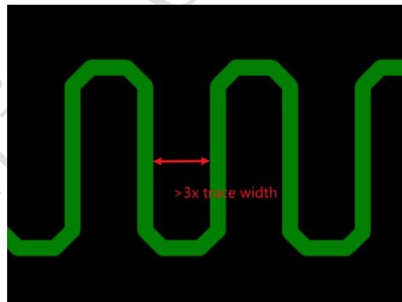
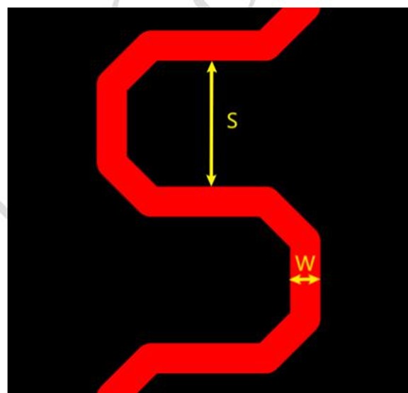
An adequate spacing should be maintained between the inside traces of a bend. Recommend 3 times the trace width or greater(S≧3W).
-
The propagation delay associated with vias should be accounted for in the trace length. The schematic of vias length is shown in the figure below.
-
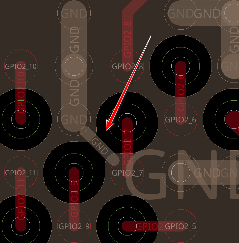
One via per GND pad of Dram chip. Add GND vias as much as possible. The schematic of the number of GND vias is shown in the figure below.
-
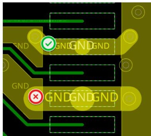
Remove unused via pads, because they cause unwanted capacitance and destroy plane.
-
Avoid making slits of plane due to the via clearance as possible. The schematic of route optimization plane slits is shown in the figure below.
-
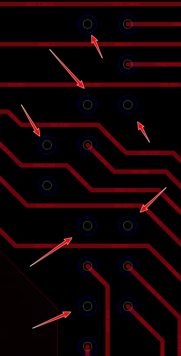
For LPDDR4/4X, VDDQLP, VDDQ, VAA power supply, it is recommended that one pin corresponds to one power via, for example as follows.
The following three pictures respectively illustrate: Requirements for the number of vias corresponding to the LPDDR4/4X chip VDDQ power pins, Requirements for the number of vias corresponding to the LPDDR4/4X chip VAA power pins, and Requirements for the number of vias corresponding to the LPDDR4/4X chip VDDQLP power pins.
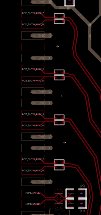
PCIe3.0 PCB Design
| Parameter | Requirement |
|---|---|
| Trace Impedance | Differential 85 to 100 ohm, with a tolerance of ±10%. Note: For the PCIe3.0 trace impedance, please refer to the schematic system design.
|
| Max Intra-pair Skew | 5Mil |
| Max trace length on carrier board |
Other applications require specific analysis. |
| Maximum allowed via | Recommended not to exceed 2 vias. |
| Airgap between Signals |
Where H represents the layer height. |
SATA3.0 PCB Design
| Parameter | Requirement |
|---|---|
| Trace Impedance | 90 to 100 ohm ±10% differential |
| Max Intra-pair Skew | 5Mil |
| Trace Length on Carrier Board | A210 to SATA hard disk interface is approximately 6dB@3GHz |
| Maximum Allowed Via | Recommend not to exceed 2 vias |
| Airgap between Signals |
Where H represents the layer height. |
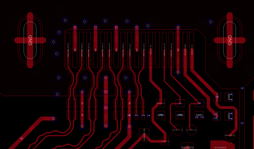
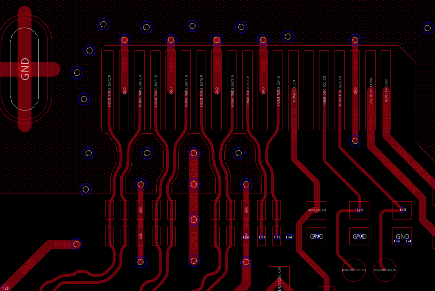
HDMI2.0 PCB Design
| Parameter | Requirement |
|---|---|
| Trace Impedance | 100 ohm, can be decreased to 90ohm |
| Propagation Delay (length) for Reference | 4 inches for top layer (can be relaxed) |
| Relative Delay (Group Skew) | 750mil |
| Static Phase (Intra-pair Skew) | 5mil |
| TVS Parasitic Capacitance | < 0.6pF for HDMI2.0 |
-
Place GND through via in BGA zone as showed below and recommend to follow routing recommendations, GND via interval length should less than 150mil.
-
If the HDMI adopts AC coupling mode (typically for applications with strict surge protection requirements), an external pull-up circuit must be added at the termination end. It is recommended that the stub length introduced by the external circuit should be less than 80 mil. For HDMI 2.0, pull-up resistor packages should ideally be 0201, and must not exceed 0402.
The HDMI2.1 BGA area fanout layout is shown in the figure below.
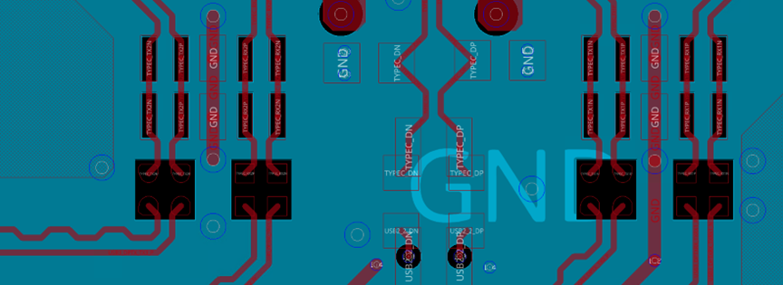
USB3.1 PCB Design
The USB3.1 layout requirements are shown in the figure below.
| Parameter | Requirement |
|---|---|
| Trace Impedance | 90ohm differential |
| Max Intra-Pair Skew | 5mil |
| Max Trace Length on Carrier Board | <5 inches M4-grade plate |
| Airgap between Signals | The inner spacing is 3xH and the outer spacing is 11xH. Where H represents the layer height |
| TVS Parasitic Capacitance | USB3.2 Gen2 10Gps: < 0.3pF |
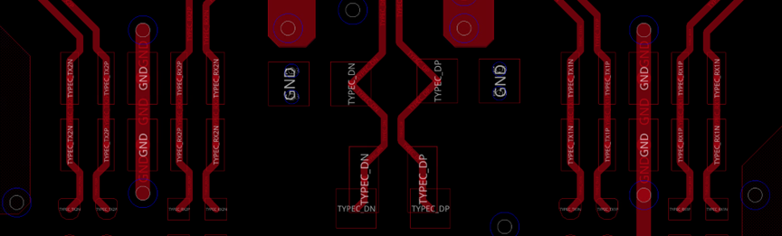
USB Type C: The DP/DN (Differential Pairs) must be interconnected on both sides (DP0/DP1) at the connector to avoid the trace stubs.
MIPI PCB Design
The MIPI-CSI layout requirements are shown in the figure below.
| Parameter | Requirement |
|---|---|
| Trace Impedance | 90ohm differential |
| Max Intra-Pair Skew | <5mil |
| Data to Clock Matching | <60mil |
| Max Trace Length on Carrier Board | <6 inches·M4-grade plate (Further evaluation is required by combining the FPC length with the application rate) |
| Maximum Allowed Via | Recommended not to exceed 4 |
| Minimum Airgap between Pair to Pair | Recommend ≥4 times the width of MIPI trace. At least 3 times the width of MIPI trace. |
| Minimum Airgap between MIPI and Other Signals | Recommend ≥4 times the width of MIPI trace. At least 3 times the width of MIPI trace. |
eMMC PCB Design
| Parameter | Requirement |
|---|---|
| Trace Impedance | 50ohm±10% single ended |
| Matching Resistors (Source End) | 22ohm, placed at a distance less than 500mil from A210 |
| Data to Clock Matching | <100mil |
| Max Trace Length | <3.5 inches |
| Minimum Airgap of eMMC Signals | At least 2 times the width of eMMC trace |
| Minimum Airgap between eMMC and Other Signals | Recommend 3 times the width of eMMC trace. At least 2 times the width of eMMC trace |
| Maximum Allowed Via | Recommend ≤2 vias |
eMMC signal should route with reference to ground plane, and place stitching via within 30mil (center-to-center) of the signal transition vias. Via-stitch should able to connect both reference plane to ensure continuous grounding.
The eMMC layout requirements are shown in the figure below.
SDIO PCB Design
The SDIO layout requirements are shown in the figure below.
| Parameter | Requirement |
|---|---|
| Trace Impedance | 50ohm ±10% single ended |
| Data to Clock Matching | < 120mil |
| Max Trace Length | The value of (PCB length (inch)× 4 + capacitance value in the circuit (pF)) should be less than <27pF. e.g. If there is a 10pF capacitance on the circuit, then the trace length must be <4 inches |
| Minimum airgap of SDMMC/SDIO Signals | At least 2 times the width of SDIO trace |
RGMII PCB Design
RGMII layout requirements are shown in the figure below.
| Parameter | Requirement |
|---|---|
| Trace Impedance | 50ohm ±10% single ended |
| Matching Resistors (Source End) | 22ohm, placed at a distance less than 500mil from A210 |
| (TXD-3, TXEN) to TXCLK 等长 Mismatch | <100mil |
| (RXD-3, RXDV) to RXCLK 等长 Mismatch | <100mil |
| Max Trace Length | < 5 inches |
| Minimum Airgap of RGMI Signals (TX or RX Signal Lines in the Same Group) | At least 2 times the width of RGMI trace. Or crosstalk levels within approximately 5% after simulation are also acceptable |
| Minimum Airgap between RGMI and Other Signals | Recommend 5 times the width of RGMII trace. At least 2 times the width of RGMI trace. or separated by GND. Notice that the proximal crosstalk between TX and RX |
| clk Trace | The clk signals recommended to be grounded |