Schematic Diagram Design Suggestions
Minimum System Design
Clock Circuit
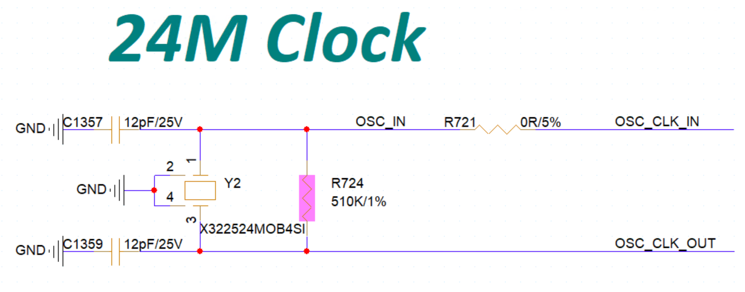
System Clock
The internal oscillator circuit of the A210 chip, together with the external 24MHz crystal, forms the system clock. A 510 kohm, 1% tolerance feedback resistor is provisioned for between the OSC_CLK_IN and OSC_CLK_OUT nets and is not populated by default.
Note:
- The selected crystal must have a drive level not exceeding 100 μW and an equivalent series resistance (ESR) of less than 80 ohm.
- The crystal load capacitors CL should be selected according to the actual crystal's CL value requirements, and the frequency tolerance at room temperature should be within 30ppm.
- The crystal CL value is 12pF selected by our company which is not a general value, and the capacitor material is recommended to use C0G or NPO.
- It is recommended to use a 4-pin surface-mounted crystal, with two GND pins fully connected to the PCB ground to enhance the clock's ability to resist ESD interference.
The system clock can also be supplied directly by an external active crystal oscillator circuit with a 1.8V clock amplitude. In this configuration, the clock signal is fed into the OSC_CLK_IN pin, while the OSC_CLK_OUT pin is left floating. The clock specifications are listed in the table below.
| Parameter | Spec. | Description | ||
|---|---|---|---|---|
| Min | Max | Unit | ||
| Frequency | 24.000000 | MHz | ||
| Frequency tolerance | ±30 | ppm | ||
| Clock amplitude | 1.8 | V | peak-to-peak | |
| Working temperature | -20 | 80 | °C | |
| ESR | / | 80 | Ohm | |
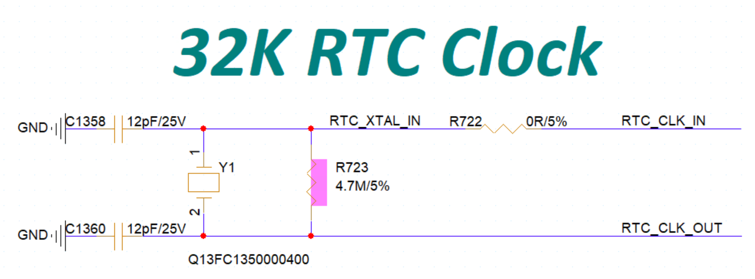
RTC Clock
The internal oscillator circuit of the A210 chip, together with the external 32.768KHz crystal, forms the RTC clock. A 4.7Mohm resistor is provisioned for between the RTC_CLK_IN and RTC_CLK_OUT nets and is not populated by default.
Note:
- The selected crystal must have a drive level not exceeding 1 μW and an equivalent series resistance (ESR) of less than 70 kohm.
- The crystal load capacitors CL should be selected according to the actual crystal's CL value requirements, and the frequency tolerance at room temperature should be within 30 ppm.
- The crystal CL value is 12pF selected by our company which is not a general value, and the capacitor material is recommended to use C0G or NPO.
The RTC clock can also be supplied directly by an external active crystal oscillator circuit with a 0.8V clock amplitude. In this configuration, the clock signal is fed into the RTC_CLK_IN pin, while the RTC_CLK_OUT pin is left floating. The clock specifications are listed in the table below.
| Parameter | Spec. | Description | ||
|---|---|---|---|---|
| Min | Max | Unit | ||
| Frequency | 32.768000 | KHz | ||
| Frequency tolerance | ±30 | ppm | ||
| Clock amplitude | 0.8 | V | peak-to-peak | |
| Duty cycle | 45 | 55 | % | |
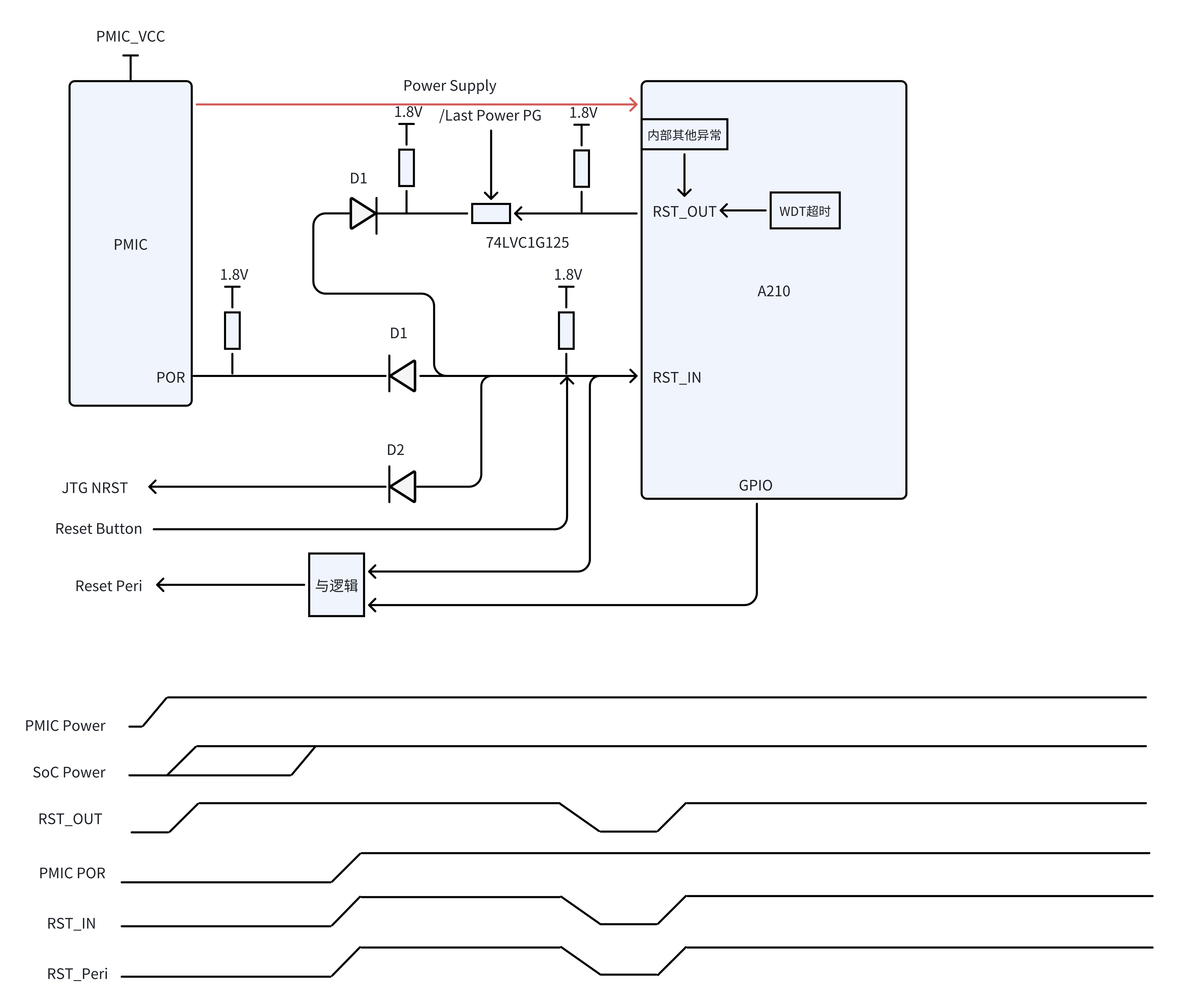
Reset/Watchdog
The reset circuit primarily involves: the reset selection pin POR_SEL (Pin E6), the reset input pin RST_N_IN (Pin D14), and the watchdog output pin RST_N_OUT (Pin F10). The functions are described in the table below.
| Pin | Pin Name | Function | Description |
|---|---|---|---|
| E6 | POR_SEL | Reset Source Selection | Select internal or external reset source during power-on.
|
| D14 | RST_N_IN | Reset Input | The chip performs a logical AND operation between RST_N_IN and the internal POR signal, and the output is used to reset the SOC. Consequently, the RST_N_IN pin can assert a reset to the A210 at any time. The duration of the POR reset is configured by the CPU_JTG_TDO pin's pull-up/pull-down setting.
|
| F10 | RST_N_OUT | Watchdog Output | RST_N_OUT signal can be connected to either the PMIC reset input or the PMIC power on/off input via logic circuitry, triggering a power cycle (power down followed by power up) of the PMIC. Normally outputs a high level. When an internal exception occurs during DVS (Dynamic Voltage Scaling) adjustment or when the internal WDT times out, the RST_N_OUT is pulled low and a full-chip reset occurs. The PMIC needs to restore all power rails to the boot-up voltage levels and then reset the chip. |
A210 System Reset Circuit Design
-
If RST_N_OUT is asserted and PMIC power cycling is not required, the following reset circuit is recommended.
Asserting a low level on Reset Button, PMIC POR, JTG NRST or RST_N_OUT will reset SoC and peripherals. The chip can individually control the peripheral reset via GPIO.
-
If RST_N_OUT is asserted, and PMIC (with dedicated reset input pin) power cycling is required, the following reset circuit and power-up/exception timing sequence are recommended.
BOOT Mode Configuration
The boot mode of the chip is configured via the BOOT_SEL[2:0] pins.

The boot mode settings are shown in the table below. In the table, 1 means 4.7 kΩ pull-up, and 0 means a 1 kΩ pull-down.
| BOOT_SEL[2] | BOOT_SEL[1] | BOOT_SEL[0] | BOOT MODE |
|---|---|---|---|
| 0 | 0 | 0 | USB Fastboot (check CCTboot first, falls back to USB Fastboot after 1-second timeout) |
| 0 | 0 | 1 | eMMC, 8 bit default |
| 0 | 1 | 0 | QSPI1 NOR Flash Boot, CS0 |
| 0 | 1 | 1 | QSPI1 NAND Flash Boot,CS0 |
| 1 | 0 | 0 | Forced CCTBoot |
| 1 | 0 | 1 | SD Card Boot, SDIO0 |
| 1 | 1 | 0 | QSPI0 NOR Flash, CS0 |
| 1 | 1 | 1 | QSPI0 NAND Flash, CS0 |
System Initialization Configuration Signals
There are several STRAP signals affect the system's boot configuration. The SoC's internal reset signal is generated by performing a logical AND operation between the RST_IN and the internal POR signals. The state of the STRAP pins is sampled approximately 4 ms after this internal reset signal is released. Therefore, the logic levels on the STRAP pins must remain stable for a window of 10 ms centered around the release of RST_IN.
The signal levels of the STRAP pins can be configured using pull-up or pull-down resistors. A 4.7 kΩ resistor is recommended for pull-up, and a 1 kΩ resistor for pull-down. The pull-up voltage source for all STRAP signals is AVDD18_AON.
TEST_MODE Pin Design
TEST_MODE pin for test mode selection.
![]()
The signal description is as follows.
| Signal | Description | Design Recommendation |
|---|---|---|
| TEST_MODE | TEST Mode selection pin. 0: Normal mode,1: Test mode. | Pull-down. Normal mode by default. |
POR_SEL Pin Design
POR_SEL pin for selecting between the internal and external Power-On Reset (POR) sources.
![]()
The signal description is as follows.
| Signal | Description | Design Recommendation |
|---|---|---|
| POR_SEL | POR selection pin. 0: External POR source. 1: Internal POR source. | Reserve a pull-up resistor footprint but leave it unpopulated (DNP). Internal pull-down resistor is integrated. Internal POR is disabled by default. |
DEBUG_MODE Pin Design
DEBUG_MODE pin for debug mode selection.
![]()
The signal description is as follows.
| Signal | Description | Design Recommendation |
|---|---|---|
| DEBUG_MODE | DEBUG Mode selection pin. 0: Normal mode. 1: Debug mode. | Pull down to GND. Normal mode by default. |
MCM_EN & MCM_CHIP_ID Pin Design
MCM_EN pin indicates whether the chip is a single-die or multi-die configuration.
![]()
MCM_CHIP_ID[1:0] pin for CHIP ID identification.
The signal description is as follows.
| Signal | Description | Design Recommendation |
|---|---|---|
| MCM_EN | Indicates single-die or multi-die configuration. The BootROM executes different boot sequences based on this signal level. For single-die designs, pull this signal low. (The D2D (Die-to-Die) function for single-die chips can also be enabled via software configuration.) | Pull down for single-die. Pull up for multi-die. |
| MCM_CHIP_ID[1:0] | Represents the Chip ID in multi-die configurations. | Adopt pull-up or pull-down resistors respectively according to the Chip ID requirements. |
Note:
In multi-die configurations, the following IO functions are fixed and cannot be modified.
GPIO Fixed Function (Non-configurable in Multi-die) AOGPIO1_0 MCM_CHIP_ID0 AOGPIO1_1 MCM_TIM_TICK AOGPIO1_6 AO12C2_SCL AOGPIO1_7 AO12C2_SDA AOGPIO1_9 MCM_CHIP_ID1 GPIO0_14 OCD_RESP1 GPIO0_15 OCD_RESP2 GPIO0_16 OCD_RESP3 GPIO0_17 OCD_CMD GPIO1_16 OCD_CLK
PCIEX4_TYPE Pin Design
PCIEX4_TYPE pin for PCIE mode selection.
![]()
The signal description is as follows.
| Signal | Description | Design Recommendation |
|---|---|---|
| PCIEX4_TYPE | PCIE TYPE selection. 0: EP. 1: RC. | Configure as needed. |
CPU_JTG_TDO Pin Design
During power-on, CPU_JTG_TDO pin for internal POR duration selection.
![]()
The signal description is as follows.
| Signal | Description | Design Recommendation |
|---|---|---|
| CPU_JTG_TDO | POR duration selection. 0:20ms. 1:80ms. | Reserve a pull-up resistor footprint but leave it DNP. Internal pull-down resistor is integrated. 20 ms reset duration by default. |
JTAG and UART Debug Circuit
CPU core can be accessed via an emulator. It is recommended to reserve a JTAG circuit to facilitate debugging. Refer to the following circuit reference.
JTAG design recommendation is shown in the figure below.
| NO. | Recommended Design | Remarks |
|---|---|---|
| 1 | E902, C908, and C920 shares a single CPU JTAG debug interface. | CPU JTAG IO reside in the AVDD18_AON power domain. |
| 2 | For TCLK, reserve a 10 kΩ pull-up resistor (DNP by default). | |
| 3 | For TMS, reserve a 10 kΩ pull-up resistor (DNP by default). | |
| 4 | For TDI, reserve a 10 kΩ pull-up resistor (DNP by default). | |
| 5 | For TDO, the chip has an internal pull-down; reserve an external pull-up resistor (DNP by default). | |
| 6 | For TRST, the chip has an internal pull-up; reserve an external 10 kΩ pull-up resistor (DNP by default). | |
| 7 | Used for system reset. Can be connected to the system reset input via a diode. | |
| 8 | JTAG VREF power supply: 1.8V. Reserve a 0 Ω resistor footprint. If leakage occurs, replace it with a Schottky diode or a high-value resistor. | |
| 9 | All JTAG signal connectors need to be placed close to ESD protection devices. |
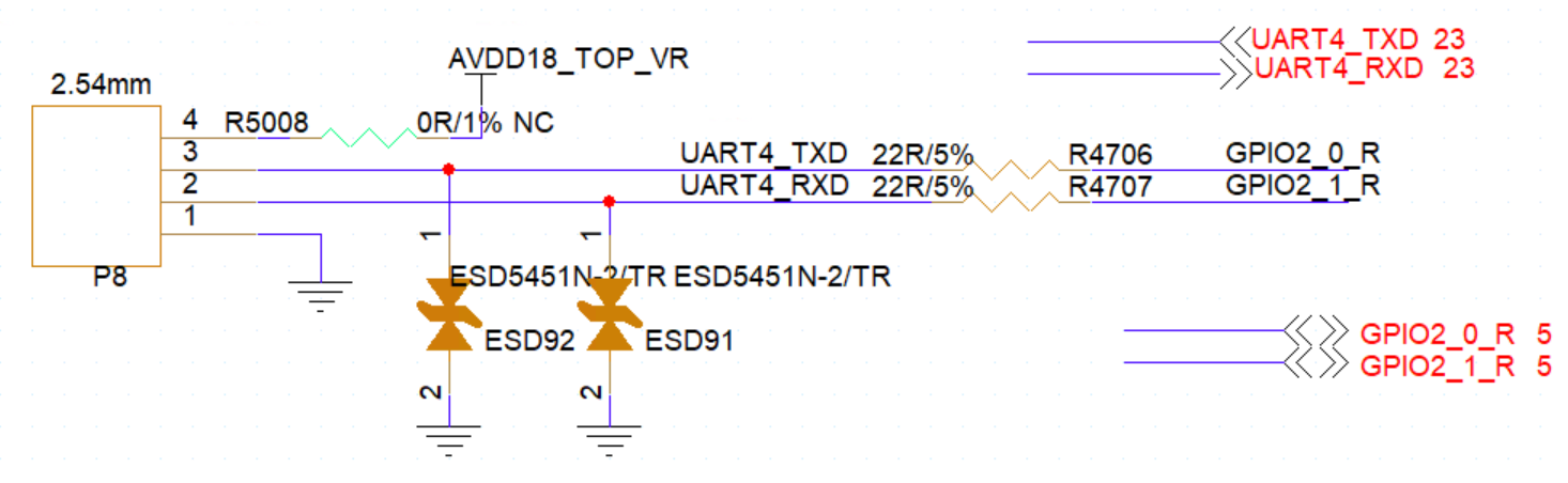
A210 UART debug is mainly divided into the E902 debug port (using AOUART) and the C908/C920 debug port (using UART4).


To enhance ESD and surge resistance and prevent damage to pins during development, add TVS diodes to the UART interface. It is recommended to reserve 2.54 mm pitch headers. If space is limited, use test points with a diameter of at least 0.7 mm to facilitate soldering.
DDR Circuit
DDR Controller Introduction
The DDR Controller interface compliant with JEDEC SDRAM standards. The key features are as follows.
- Compatibility with LPDDR4/LPDDR4X standards.
- Up to 2 ranks.
- Supports 2 channels, each with a 32-bit width.
- Supports DDR4 3200 Mbps.
- LPDDR4/4x speed: supports up to 4266Mbps.
- Supports Error Correction Code (ECC).
- DDR4 with a maximum capacity of 16GB.
- LPDDR4/4x with a maximum capacity of 16GB.
- UDIMM is not supported.
Circuit Design Recommendations
Please notice that the DDR PHY and each DRAM chip's schematic diagrams need to be consistent with the reference design, including decoupling capacitors.
The chip supports DDR4, LPDDR4, and LPDDR4X, each with different I/O signals. Accordingly, please select the signals corresponding to the DRAM type and refer to the respective DRAM reference designs.
Design Constraints.
- The sequence of DQ and CA signals must be assigned according to the reference design. Trace routing must directly follow our company's Demo. Modifications are not permitted.
- The DDR PHY ZQ pin must be connected to a 240-ohm (1%) resistor tied to the DVDD06_DDR_VDDQLP power supply.
DDR Chip Peripheral Circuit Design
- The ZQ pin on the LPDDR4/4x chip must be connected to a-240 ohm (1%) resistor tied to DVDD06_DDR_VDDQLP.
- The ODT_CA pin on the LPDDR4/4x chip must be connected to a 10 Kohm (5%) resistor tied to DVDD11_DDR_VDDQ.
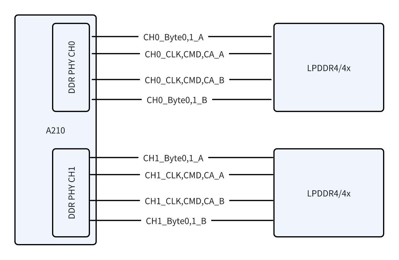
DDR Topology and Matching Design
-
In dual 32-bit LPDDR4/4x mode, point-to-point topology is adopted for DQ/CA signals.
-
In single 32-bit LPDDR4/4x mode, only connect to DDR PHY CH0.
DDR Power Design
A210 DDR PHY power supply requirement summary is as follows.
| DDR PHY POWER | Min(V) | Typ(V) | Max(V) | |
|---|---|---|---|---|
| DDR PLL POWER | DVDD08_PLL | 0.72 | 0.8 | 0.96 |
| AVDD18_PLL | 1.62 | 1.8 | 1.98 | |
| DDR_PHY | DVDD_DDR | 0.74 | 0.8 | 0.88 |
| AVDD12_DDR_VDDQ_0 | 1.14/1.06 | 1.2/1.1 | 1.26/1.17 | |
| AVDD06_DDR_VDDQLP_0 | 0.57 | 0.6 | 0.65 | |
| AVDD18_DDR_VAA_0 | 1.67 | 1.8 | 1.98 | |
| AVDD12_DDR_VDDQ_1 | 1.14/1.06 | 1.2/1.1 | 1.26/1.17 | |
| AVDD06_DDR_VDDQLP_1 | 0.57 | 0.6 | 0.65 | |
| AVDD18_DDR_VAA_1 | 1.67 | 1.8 | 1.98 |
LPDDR4/4x chip power supply requirement summary is as follows.
| DDR Chip POWER | LPDDR4 | LPDDR4x | |
|---|---|---|---|
| Core power 1 | VDD1 | 1.8 | 1.8 |
| Core power 2 | VDD2 | 1.1 | 1.1 |
| IO Buffer Power | VDDQ | 1.1 | 0.6 |
Note:
All voltage values listed in the tables above represent Typical (Typ) values.
eMMC Circuit
eMMC Controller Introduction
A210 provides one eMMC controller with the following features.
- Compliant with eMMC 5.0 and 5.1 specifications.
- Supports 1-bit, 4-bit, and 8bit data bus widths.
- Supports HS400 mode, and backward compatible with HS200 and DDR52 modes.
The boot mode is configured via BOOT_SEL[2:0], as shown below.
| BOOT_SEL[2] | BOOT_SEL[1] | BOOT_SEL[0] | BOOT MODE |
|---|---|---|---|
| 0 | 0 | 1 | eMMC, 8 bit default |
eMMC Circuit Design Recommendations
Please follow the reference schematic for eMMC signal connections, including the decoupling capacitors for each power rail.
eMMC Topology and Matching Design
The external signal connections for eMMC are shown in the figure below.
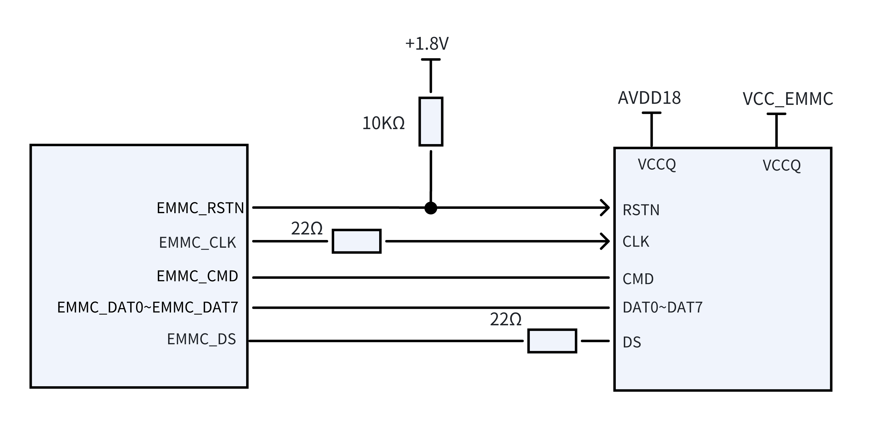
The recommended eMMC interface matching design is shown in the table below.
| Signal | Design Recommendation |
|---|---|
| EMMC_CLK | Place a 22 Ω series resistor at the SoC side. Trace length must not exceed 2 inches. |
| EMMC_CMD | Direct connection. Trace length must not exceed 2 inches. |
| EMMC_DAT0~7 | Direct connection. Trace length must not exceed 2 inches. |
| EMMC_DS | Place a 22 Ω series resistor at the eMMC side. Trace length must not exceed 2 inches. If the eMMC device lacks a DS pin, leave the SoC EMMC_DS pin floating (NC). |
| EMMC_RSTN | Direct connection with a 10 kΩ pull-up resistor. |
eMMC Power-up Requirements
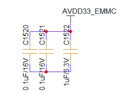
For eMMC interface, there are AVDD33_EMMC and AVDD18_EMMC power rails. The power requirements are as follows.
| eMMC PHY POWER | Min (V) | Typ (V) | Max (V) | |
|---|---|---|---|---|
| CORE | DVDD08_TOP | 0.72 | 0.8 | 0.88 |
| VDDIO33 | AVDD33_EMMC | 2.97 | 3.3 | 3.63 |
| VDDIO18 | AVDD18_EMMC | 1.62 | 1.8 | 1.98 |
QSPI Flash Circuit
QSPI Flash (Boot Support) Introduction
A210 chip provides two QSPI controllers used for QSPI devices with the following key features.
- Support for serial NOR Flash and serial Nand Flash.
- Support for 1-line, 2-line, and 4-line modes.
When QSPI0/1 is connected to Nor Flash or NAND Flash, the boot mode is configured via BOOT_SEL[2:0] as shown in the table below.
| BOOT_SEL[2] | BOOT_SEL[1] | BOOT_SEL[0] | BOOT MODE |
|---|---|---|---|
| 0 | 1 | 0 | QSPI1 NOR Flash Boot, CS0 |
| 0 | 1 | 1 | QSPI1 NAND Flash Boot,CS0 |
| 1 | 1 | 0 | QSPI0 NOR Flash, CS0 |
| 1 | 1 | 1 | QSPI0 NAND Flash, CS0 |
QSPI Flash Circuit Design Recommendation
Please follow the reference design schematic for FSPI Flash signals connections, including the decoupling capacitors for each power rail.
QSPI Flash Topology and Matching Design
The connection diagram for a single SPI Flash device is shown below (QSPI0 as an example). The configuration for QSPI1 is similar.
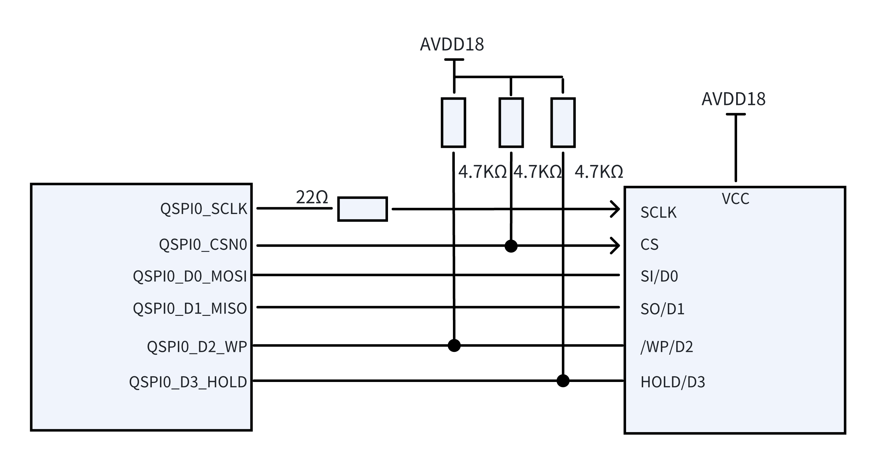
QSPI interface design recommendations are shown in the table below.
| Signal | Design Recommendation |
|---|---|
| QSPI0_SCLK | Place a 22 Ω series resistor at the SoC side. Trace length must not exceed 2 inches. |
| QSPI0_CSN0 | Direct connection. QSPI0_D2_WP, QSPI0_D3_HOLD, and QSPI0_CSN0 require pull-up resistors (typically 4.7 kΩ). Trace length must not exceed 2 inches. |
| QSPI0_D0_MOSI | |
| QSPI0_D1_MISO | |
| QSPI0_D2_WP | |
| QSPI0_D3_HOLD | |
| QSPI1_SCLK | Place a 22 Ω series resistor at the SoC side. Trace length must not exceed 2 inches. |
| QSPI1_CSN0 | Direct connection. QSPI1_D2_WP, QSPI1_D3_HOLD, and QSPI1_CSN0 require pull-up resistors (typically 4.7 kΩ). Trace length must not exceed 2 inches. |
| QSPI1_D0_MOSI | |
| QSPI1_D1_MISO | |
| QSPI1_D2_WP | |
| QSPI1_D3_HOLD |
QSPI Power-up Requirements
The A210 FSPI Flash interface implements a single power supply and has no specific power-up sequencing requirements.
The SPI Flash has only one 1V8 power supply. Ensure level matching between the SoC and the Flash device.
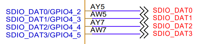
SDIO Interface
SDIO Interface (Boot Support) Introduction
A210 chip provides one SDIO controller used for SDIO device with the following key features.
- Supports SD3.0/SDIO3.0.
- Supports SDR12/SDR25/SDR50/SDR104 mode.
- Support for 1-bit/4-bit data bus widths.
- Supports voltage switching between 3.3 V and 1.8 V.
When an external SD card is connected, the boot mode is configured via BOOT_SEL[2:0] as shown in the table below.
| BOOT_SEL[2] | BOOT_SEL[1] | BOOT_SEL[0] | BOOT MODE |
|---|---|---|---|
| 1 | 0 | 1 | SD Card Boot, SDIO0 |
SD Card Circuit Design Recommendations
Please follow the reference design schematic for SDIO signals connections, including the decoupling capacitors for each power rail.
SD Card Topology and Matching Design
When an external SD card is connected, the reference design schematic is as follows.
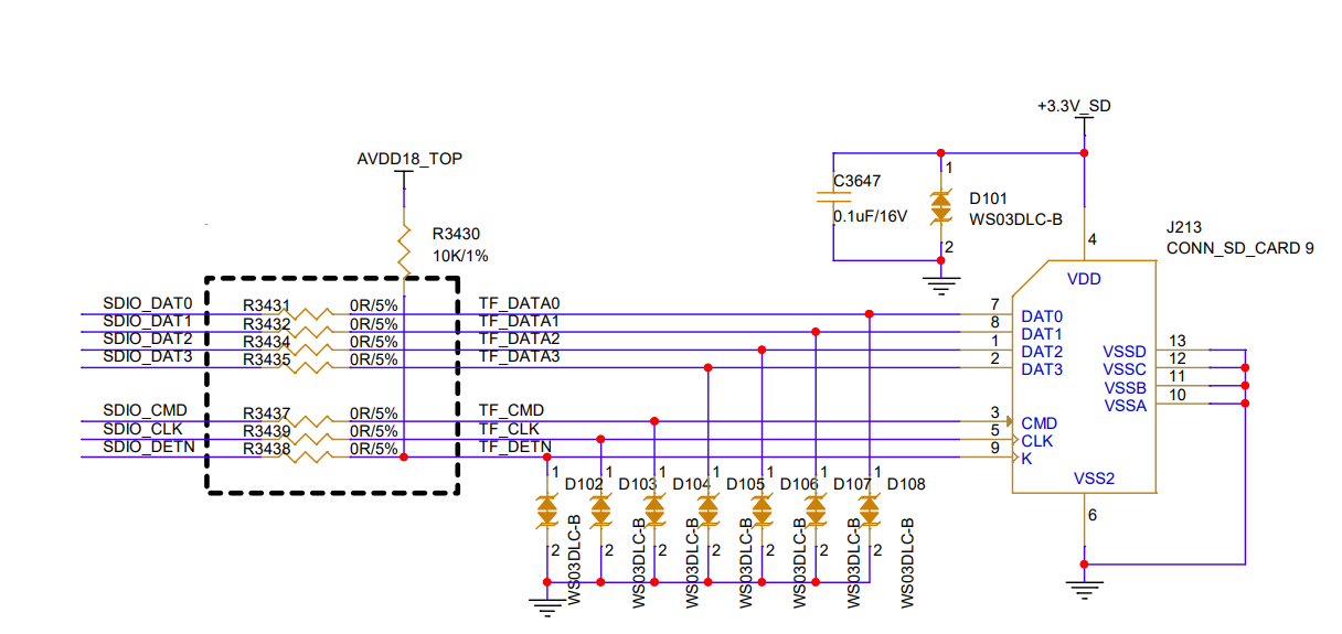
The recommended SD Card interface matching design is shown in the table below.
| Signal | Design Recommendation |
|---|---|
| SDIO0_CLK | Place a 22 Ω series resistor at the SoC side. The resistor should be located within 0.6 inches of the source, and the total trace length must not exceed 4 inches. |
| SDIO0_CMD | Trace length must not exceed 4 inches. |
| SDIO0_DAT0~3 | Place a 22 Ω series resistor at the SoC side. The resistor should be located within 1 inch of the source. |
| SD Card Power Enable | Since SD cards lack a dedicated reset signal, a power cycle (power off and on) is required to reset the card. Use a GPIO to control the power supply switching. |
Design Considerations for SDIO Wi-Fi Modules
When the SDIO interface connecting to a Wi-Fi module, please strictly refer to the followings.
- Ensure the I/O voltage levels of the module match the SoC. Use level shifters if the voltages are inconsistent.
- Select the load capacitors based on the crystal's rated CL value. Ensure the frequency tolerance remains within ±10 ppm at room temperature.
- Reserve a π-type matching network circuit for antenna tuning and optimization.
GPIO Circuit
All GPIO operates at a voltage of 1.8V. Signals named AOGPIOx_x, whose power domain is AVDD18_AON, are Always-On (AON) GPIOs and can be used as wake-up interfaces.
Power Supply Design
A210 Power Supply Introduction
A210 Power Supply Requirements
| Module | Pin | Power Description |
|---|---|---|
| TOP | DVDD08_TOP | TOP digital logic supply for TOP, covers: VI, VO, USB, PCIe, PERI 1/2/3, ADC, and VT sensor. |
| AVDD18_TOP | Peri 1/2 PAD, ADC, and VT sensor. | |
| C902 | DVDD08_AON | AON digital logic supply, covers: POR and RC. |
| AVDD18_AON | AON PAD, POR, RC. | |
| CPU | DVDD_CPU | Digital logic supply for CPU_SS/C908. |
| DVDM_CPU | MEM supply for CPU_SS/C908. | |
| DVDD_CPU_P | Digital logic supply for C920. | |
| GPU | DVDD_GPU | Digital logic supply for GPU_SS. |
| NPU | DVDD_NPU | Top-level digital logic supply for NPU_SS. |
| DVDD_NPU_VIP | Computing core digital supply for NPU_SS, covers: SLICE A/B/C and PPP. | |
| PLL | DVDD08_PLL | Digital logic supply for all PLLs. |
| AVDD18_PLL | Analog circuit supply for all PLLs. | |
| VP | DVDD_VP | Digital logic supply for VP_SS, covers: VENC, VDEC and G2D. |
| DDR | DVDD08_DDR | Digital logic supply for DDR_SS, covers: DDR CTRL and SLC. |
| DDR_PHY | AVDD12_DDR_VDDQ_0 | DDR PHY IO supply. |
| AVDD12_DDR_VDDQ_1 | ||
| AVDD06_DDR_VDDQLP_0 | DDR PHY IO supply. | |
| AVDD06_DDR_VDDQLP_1 | ||
| AVDD18_DDR_VAA_0 | DDR PHY PLL supply. | |
| AVDD18_DDR_VAA_1 | ||
| MIPI_PHY | AVDD08_MIPI | 0.8V analog circuit supply for MIPI CSIO/1/2/3, MIPI DSI, and HDMI PHY. |
| AVDD18_MIPI | 1.8V analog circuit supply for MIPI CSIO/1/2/3, MIPI DSI, and HDMI PHY. | |
| USB2_PHY | DVDD08_USB2 | 0.8V digital logic supply for USB2.0 0/1/2. |
| AVDD33_USB2 | 3.3V analog circuit supply for USB2.0 0/1/2. | |
| AVDD18_USB2 | 1.8V analog circuit supply for USB2.0 0/1/2. | |
| USB31_PHY | AVDD08_USB3 | 0.8V analog circuit supply for USB3.1. |
| AVDD18_USB3 | 1.8V analog circuit supply for USB3.1. | |
| PCIE_PHY | AVDD08_PCIE3 | 0.8V analog circuit supply for PCIe0/1. |
| AVDD18_PCIE3 | 1.8V analog circuit supply for PCIe0/1. | |
| EMMC_PHY | AVDD33_EMMC | 3.3V analog circuit supply for eMMC/SD. |
| AVDD18_EMMC | 1.8V analog circuit supply for eMMC/SD. | |
| EFUSE_QPS | AVDD18_EFUSE | Flashing supply for EFUSE. |
| D2D_PHY | DVDD08_D2D | D2D digital logic supply. |
| AVDD18_D2D | 1.8V analog circuit supply for eMMC/SD. | |
| AVDD08_D2D | 0.8V analog circuit supply for eMMC/SD. | |
| VSS | VSS | Digital ground (GND). |
| AVSS_PLL | AVSS_PLL | PLL ground (GND). |
Note: If Die-to-Die (D2D) applications are not used, the D2D_PHY power pins can be connected to GND.
A210 Power Up/Down Timing Requirements
| Power Up | Power Down | Power Pin |
|---|---|---|
| 1 | 13 | AVDD18_AON |
| 2 | 12 | DVDD08_AON |
| 3 | 11 | AVDD18_TOP |
| 4 | 10 | DVDD08_PLL |
| 4 | 10 | DVDD08_TOP |
| 4 | 10 | AVDD08_USB3 |
| 4 | 10 | AVDD08_PCIE3 |
| 4 | 10 | DVDD08_USB2 |
| 5 | 9 | AVDD18_EMMC |
| 5 | 9 | AVDD18_USB2 |
| 6 | 8 | AVDD33_EMMC |
| 6 | 8 | AVDD33_USB2 |
| 7 | 7 | DVDD08_DDR |
| 8 | 6 | DVDD11_DDR_VDDQ |
| 9 | 5 | DVDD06_DDR_VDDQLP |
| 10 | 4 | DVDD18_DDR_VAA |
| 11 | 3 | DVDD_CPU |
| 12 | 2 | DVDDM_CPU |
| 13 | 1 | POR release |
Note:
- Please ensure that DVDD08_PLL, DVDD08_TOP, AVDD08_USB3, AVDD08_PCIE3 and DVDD08_USB2 maintains power-up/down simultaneously. (These power rails can be merged.)
- The minimum system has strict power sequencing requirements. Theoretically, there are no specific timing constraints between different analog PHY modules. After the last voltage has stabilized, the POR must be held for at least 10ms before release.
The recommended typical power-up/down sequence for each module is as follows:
-
DDR_PHY
Although the DDR PHY has no inherent timing requirements, most designs share power rails between the PHY and the DDR devices. In such cases, the design must follow the power-up and power-down sequences specified for the DRAM devices.
Related Timing SOC_DDR Power Pin DDR Chip Power Pin 1 AVDD18_DDR_VAA VDD1 2 AVDD12_DDR_VDDQ0/1 VDD2 3 AVDD06_DDR_VDDQLP0/1 VDDQ -
CPU
The power-up sequence for the CPU is as follows. The power-down sequence follows the reverse order.
Related Timing SOC_CPU Power Pin 1 DVDD_CPU 2 DVDM_CPU 3 DVDD_CPU_P -
MIPI_PHY
The power-up sequence for the MIPI_PHY is as follows. The power-down sequence follows the reverse order.
Related Timing SOC_MIPI Power Pin 1 AVDD08_MIPI 2 AVDD18_MIPI -
PCIE_PHY
The power-up sequence for the PCIE_PHY is as follows. The power-down sequence follows the reverse order.
Related Timing SOC_PCIE Power Pin 1 AVDD08_PCIE3 2 AVDD18_PCIE3 -
USB2_PHY
The power-up sequence for the USB2_PHY is as follows. The power-down sequence follows the reverse order.
Related Timing SOC_USB2 Power Pin 1 DVDD08_USB2 2 AVDD18_USB2 3 AVDD33_USB2 -
EMMC_PHY
The power-up sequence for the EMMC_PHY is as follows. The power-down sequence follows the reverse order.
Related Timing SOC_PCIE Power Pin 1 AVDD08_PCIE3 2 AVDD18_PCIE3
Note:
Modules not explicitly listed do not have specific timing requirements. However, all modules must generally comply with the power-up and power-down sequences of the minimum system.
Power Design Recommendations
Power-On and Standby Circuitry Solutions
For the first power-on, the power requirements for each module are as follows.
| Module | Pins | First Power-On Supply Requirements |
|---|---|---|
| TOP | DVDD08_TOP | Must be powered |
| AVDD18_TOP | Must be powered | |
| AON | DVDD08_AON | Must be powered |
| AVDD18_AON | Must be powered | |
| CPU | DVDD_CPU | Must be powered |
| DVDM_CPU | Must be powered | |
| DVDD_CPU_P | Not required to be powered | |
| GPU | DVDD_GPU | Not required to be powered |
| NPU | DVDD_NPU | Not required to be powered |
| DVDD_NPU_VIP | Not required to be powered | |
| PLL | DVDD08_PLL | Must be powered |
| AVDD18_PLL | Must be powered | |
| VP | DVDD_VP | Not required to be powered |
| DDR | DVDD08_DDR | Must be powered |
| DDR_PHY | AVDD12_DDR_VDDQ_0 | Not required to be powered |
| AVDD12_DDR_VDDQ_1 | Not required to be powered | |
| AVDD06_DDR_VDDQLP_0 | Not required to be powered | |
| AVDD06_DDR_VDDQLP_1 | Not required to be powered | |
| AVDD18_DDR_VAA_0 | Not required to be powered | |
| AVDD18_DDR_VAA_1 | Not required to be powered | |
| MIPI_PHY | AVDD08_MIPI | Not required to be powered |
| AVDD18_MIPI | Not required to be powered | |
| USB2_PHY | DVDD08_USB2 | Must be powered |
| AVDD33_USB2 | Must be powered | |
| AVDD18_USB2 | Must be powered | |
| USB31_PHY | AVDD08_USB3 | Must be powered |
| AVDD18_USB3 | Not required to be powered | |
| PCIE_PHY | AVDD08_PCIE3 | Must be powered |
| AVDD18_PCIE3 | Not required to be powered | |
| EMMC_PHY | AVDD33_EMMC | Must be powered |
| AVDD18_EMMC | Must be powered | |
| EFUSE_QPS | AVDD18_EFUSE | Not required to be powered |
| D2D_PHY | DVDD08_D2D | Not required to be powered |
| AVDD18_D2D | Not required to be powered | |
| AVDD08_D2D | Not required to be powered | |
| VSS | VSS | Must be powered |
| AVSS_PLL | AVSS_PLL | Must be powered |
The chip supports the low-power standby solution. When entering the standby mode, the following table shows the power supply and power-off conditions.
| Module | Pins | Deepsleep | Standby |
|---|---|---|---|
| TOP | DVDD08_TOP | Not required to be powered | Need to be powered |
| AVDD18_TOP | Not required to be powered | Need to be powered | |
| AON | DVDD08_AON | Need to be powered | Need to be powered |
| AVDD18_AON | Need to be powered | Need to be powered | |
| CPU | DVDD_CPU | Not required to be powered | Need to be powered |
| DVDM_CPU | Not required to be powered | Need to be powered | |
| DVDD_CPU_P | Not required to be powered | Not required to be powered | |
| GPU | DVDD_GPU | Not required to be powered | Not required to be powered |
| NPU | DVDD_NPU | Not required to be powered | Not required to be powered |
| DVDD_NPU_VIP | Not required to be powered | Not required to be powered | |
| PLL | DVDD08_PLL | Not required to be powered | Need to be powered |
| AVDD18_PLL | Not required to be powered | Need to be powered | |
| VP | DVDD_VP | Not required to be powered | Not required to be powered |
| DDR | DVDD08_DDR | Not required to be powered | Need to be powered |
| DDR_PHY | AVDD12_DDR_VDDQ_0 | Need to be powered | Need to be powered |
| AVDD12_DDR_VDDQ_1 | Need to be powered | Need to be powered | |
| AVDD06_DDR_VDDQLP_0 | Not required to be powered | Need to be powered | |
| AVDD06_DDR_VDDQLP_1 | Not required to be powered | Need to be powered | |
| AVDD18_DDR_VAA_0 | Not required to be powered | Need to be powered | |
| AVDD18_DDR_VAA_1 | Not required to be powered | Need to be powered | |
| MIPI_PHY | AVDD08_MIPI | Not required to be powered | Not required to be powered |
| AVDD18_MIPI | Not required to be powered | Not required to be powered | |
| USB2_PHY | DVDD08_USB2 | Not required to be powered | Need to be powered |
| AVDD33_USB2 | Not required to be powered | Need to be powered | |
| AVDD18_USB2 | Not required to be powered | Need to be powered | |
| USB31_PHY | AVDD08_USB3 | Not required to be powered | Need to be powered |
| AVDD18_USB3 | Not required to be powered | Need to be powered | |
| PCIE_PHY | AVDD08_PCIE3 | Not required to be powered | Need to be powered |
| AVDD18_PCIE3 | Not required to be powered | Need to be powered | |
| EMMC_PHY | AVDD33_EMMC | Not required to be powered | Not required to be powered |
| AVDD18_EMMC | Not required to be powered | Not required to be powered | |
| EFUSE_QPS | AVDD18_EFUSE | Not required to be powered | Not required to be powered |
| D2D_PHY | DVDD08_D2D | Not required to be powered | Not required to be powered |
| AVDD18_D2D | Not required to be powered | Not required to be powered | |
| AVDD08_D2D | Not required to be powered | Not required to be powered | |
| VSS | VSS | Need to be powered | Need to be powered |
| AVSS_PLL | AVSS_PLL | Need to be powered | Need to be powered |
Note:
In Deepsleep mode, wake-up is only supported via AON_GPIO and AON RTC. In Standby mode, the system additionally supports wake-up from USB, PCIe, and standard GPIOs (those other than AON_GPIO).
TOP Power
A210 chip's TOP power includes two parts: DVDD08_TOP and AVDD18_TOP.
The details of A210 USB2 power are as follows.
| Power | Deepsleep | Vboot(V) | Peak Current(mA) |
|---|---|---|---|
| DVDD08_TOP | Not required to be powered | 0.8 | 2151.75 |
| AVDD18_TOP | Not required to be powered | 1.8 | 400 |
-
AVDD18_TOP provides power to ADC, an LDO for power supply is recommended.
-
In the reference design schematic, DVDD08_TOP is combined with DVDD08_USB2, DVDD08_PLL, AVDD08_USB3, AVDD08_MIPI and AVDD08_PCIE. For DVDD08_TOP, refer to the decoupling capacitor diagram below (representing the total count after board-level power rail combining).
-
Place one 1uF and three 0.1uF capacitors close to the AVDD18_TOP pins. For DVDD18_TOP, refer to the decoupling capacitor diagram below.
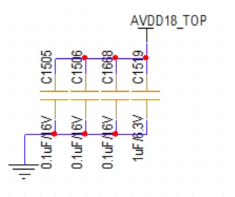
Note:
Since DVDD08_TOP is combined with multiple power supply in the reference design, therein 1 uF capacitors are allocated to the other combined power rails. However, the total count remains unchanged.
PLL Power
A210 chip's PLL power includes two parts: DVDD08_PLL and AVDD18_PLL. The details of A210 PLL power are as follows.
| Power | Deepsleep | Vboot(V) | Peak Current(mA) |
|---|---|---|---|
| DVDD08_PLL | Not required to be powered | 0.8 | 14.25 |
| AVDD18_PLL | Not required to be powered | 1.8 | 90.27 |
- An LDO for AVDD18_PLL power supply is recommended.
- DVDD08_PLL has simultaneous power-up/down requirements. In the reference design schematic, DVDD08_PLL is combined with DVDD08_TOP, DVDD08_USB2, AVDD08_USB3, AVDD08_MIPI and AVDD08_PCIE power supply. Place one 1uF capacitor close to the DVDD08_PLL pins.
- Place two 0.1uF capacitors close to the AVDD18_PLL pins.
USB2 Power
A210 chip's USB2 power includes three parts: DVDD08_USB2, AVDD18_USB2 and AVDD33_USB2. The details of A210 USB2 power are as follows.
| Power | Deepsleep | Vboot(V) | Peak Current(mA) |
|---|---|---|---|
| DVDD08_USB2 | Not required to be powered | 0.8 | 36.53 |
| AVDD18_USB2 | Not required to be powered | 1.8 | 58.68 |
| AVDD33_USB2 | Not required to be powered | 3.3 | 10.53 |
-
LDOs for AVDD18_USB2 and AVDD33_USB2 power supply are recommended.
-
DVDD08_USB2 has simultaneous power-up/down requirements. In the reference design schematic, DVDD08_USB2 is combined with DVDD08_TOP, DVDD08_PLL, AVDD08_USB3, AVDD08_MIPI and AVDD08_PCIE power supply. Place one 1uF capacitor close to the DVDD08_USB2 pins.
-
In the reference design schematic, AVDD18_USB2 is combined with AVDD18_EMMC power supply. Place one 1uF capacitor close to the AVDD18_USB2 pins. For AVDD18_USB2, refer to the decoupling capacitor diagram below.
-
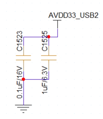
Place one 1uF and one 0.1 uF capacitors close to the AVDD33_USB2 pins. For AVDD33_USB2, refer to the decoupling capacitor diagram below.
USB3 Power
A210 chip's USB3 power includes two parts: AVDD08_USB3 and AVDD18USB3.
| Power | Deepsleep | Vboot(V) | Peak Current(mA) |
|---|---|---|---|
| AVDD08_USB3 | Not required to be powered | 0.8 | 119.4 |
| AVDD18_USB3 | Not required to be powered | 1.8 | 30.38 |
- An LDO for AVDD18_USB3 power supply is recommended.
- In the reference design schematic, AVDD08_USB3 is combined with DVDD08_TOP, DVDD08_USB2, DVDD08_PLL, AVDD08_MIPI and AVDD08_PCIE power supply. Place one 1uF capacitor close to the AVDD08_USB3 pins.
- In the reference design schematic, AVDD18_USB3 is combined with AVDD18_MIPI, AVDD18_EFUSE and AVDD18_PCIE power supply. Place one 1uF capacitor and one 0.1uF capacitor close to the AVDD18_USB3 pins.
EMMC Power
A210 chip's EMMC power includes two parts: AVDD18_EMMC and AVDD33_EMMC.
| Power | Deepsleep | Vboot(V) | Peak Current(mA) |
|---|---|---|---|
| AVDD18_EMMC | Not required to be powered | 1.8 | 323.4 |
| AVDD33_EMMC | Not required to be powered | 3.3 | 20.83 |
-
LDOs for AVDD18_EMMC and AVDD33_EMMC power supply are recommended.
-
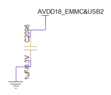
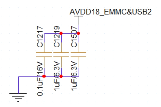
In the reference design schematic, AVDD18_EMMC is combined with AVDD18_USB2 power supply. Place two 1uF capacitors and one 0.1uF capacitor close to the AVDD18_EMMC pins. For AVDD18_EMMC, refer to the decoupling capacitor diagram below.
-
Place one 1uF capacitor and two 0.1uF capacitors close to the AVDD33_EMMC pins. For AVDD33_EMMC, refer to the decoupling capacitor diagram below.
AON Power
A210 chip's USB3 power includes two parts: AVDD18_AON and DVDD08_AON.
| Power | Deepsleep | Vboot(V) | Peak Current(mA) |
|---|---|---|---|
| DVDD08_AON | Need to be powered | 0.8 | 100 |
| AVDD18_AON | Need to be powered | 1.8 | 50 |
-
An LDO for AVDD18_AON power supply is recommended.
-
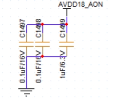
Place one 1uF capacitor and two 0.1uF capacitors close to the AVDD18_AON pins. For AVDD18_AON, refer to the decoupling capacitor diagram below.
-
Place one 1uF capacitor and two 0.1uF capacitors close to the DVDD08_AON pins. For DVDD08_AON, refer to the decoupling capacitor diagram below.
MIPI Power
A210 chip's MIPI power includes two parts: AVDD08_MIPI and AVDD18_MIPI.
| Power | Deepsleep | Vboot(V) | Peak Current(mA) |
|---|---|---|---|
| AVDD08_MIPI | Not required to be powered | 0.8 | 144.3 |
| AVDD18_MIPI | Not required to be powered | 1.8 | 43.86 |
-
An LDO for AVDD18_MIPI power supply is recommended.
-
In the reference design schematic, AVDD08_MIPI is combined with DVDD08_USB2, DVDD08_PLL, AVDD08_USB3, DVDD08_TOP and AVDD08_PCIE power supply. Place one 1uF capacitor and two 0.1uF capacitors close to the AVDD08_MIPI pins. For AVDD08_MIPI, refer to the decoupling capacitor diagram below.

-
In the reference design schematic, AVDD18_MIPI is combined with AVDD18_USB3, AVDD18_EFUSE and AVDD18_PCIE power supply. Place one 1uF capacitor and one 0.1uF capacitor close to the AVDD18_MIPI pins.
PCIE Power
A210 chip's PCIE power includes two parts: AVDD08_PCIE and AVDD18_PCIE.
| Power | Deepsleep | Vboot(V) | Peak Current(mA) |
|---|---|---|---|
| AVDD08_PCIE | Not required to be powered | 0.8 | 348.26 |
| AVDD18_PCIE | Not required to be powered | 1.8 | 165 |
-
An LDO for AVDD18_PCIE power supply is recommended.
-
In the reference design schematic, AVDD08_PCIE is combined with DVDD08_USB2, DVDD08_PLL, AVDD08_USB3, DVDD08_TO and AVDD08_MIPI power supply. Place one 10uF capacitor, one 1uF capacitor and two 0.1uF capacitors close to the AVDD08_PCIE pins. For AVDD08_PCIE, refer to the decoupling capacitor diagram below.

-
In the reference design schematic, AVDD18_PCIE is combined with AVDD18_USB3, AVDD18_EFUSE and AVDD18_MIPI power supply. Place one 1uF capacitor and one 0.1uF capacitor close to the AVDD18_PCIE pins.
EFUSE Power
A210 chip's EFUSE power is AVDD18_EFUSE.
| Power | Deepsleep | Vboot(V) | Peak Current(mA) |
|---|---|---|---|
| AVDD18_EFUSE | Not required to be powered | 1.8 | 6 |
- An LDO for AVDD18_EFUSE power supply is recommended.
- In the reference design schematic, AVDD18_EFUSE is combined with AVDD18_USB3, AVDD18_PCIE and AVDD18_MIPI power supply. Place one 1uF capacitor and one 0.1uF capacitor close to the AVDD18_EFUSE pins.
D2D Power
A210 chip's D2D power includes three parts: AVDD08_D2D, DVDD08_D2D and AVDD18_D2D.
For single-chip applications, D2D power supply can be connected to GND.
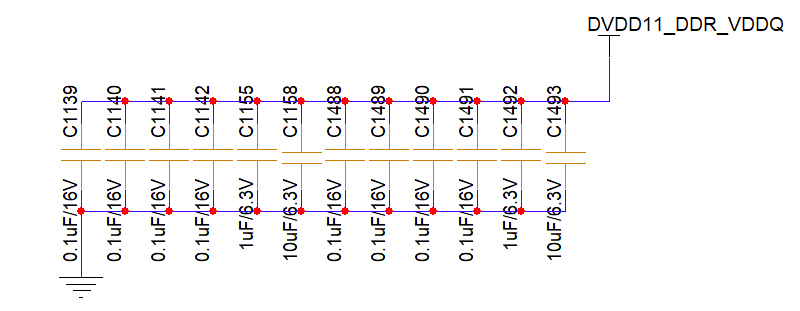
DDR Power
A210 chip's DDR power includes four parts: DVDD08_DDR, DVDD18_DDR_VAA, DVDD11_DDR_VDDQ and DVDD06_DDR_VDDQLP.
DVDD08_DDR provides power supply for the SLC (System Level Cache).
DVDD18_DDR_VAA, DVDD11_DDR_VDDQ, and DVDD06_DDR_VDDQLP provide combined power supply for both the SoC DDR controller and the DDR chips. For the details on DDR chip side, refer to the DDR Circuit.
| Power | Deepsleep | Vboot(V) | Peak Current(mA) |
|---|---|---|---|
| DVDD08_DDR | Not required to be powered | 0.8 | 2193 |
| DVDD18_DDR_VAA | Not required to be powered | 1.8 | 300 |
| DVDD11_DDR_VDDQ | Need to be powered | 1.1 | 2017.28 |
| DVDD06_DDR_VDDQLP | Not required to be powered | 0.6 | 1250 |
-
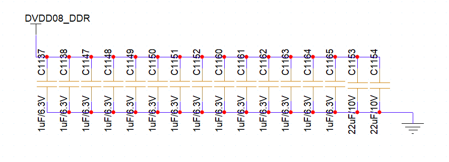
Place fourteen 1uF capacitor and two 22uF capacitors close to the DVDD08_DDR pins. For DVDD08_DDR, refer to the decoupling capacitor diagram below.
-
Place two 1uF capacitor and two 0.1uF capacitors close to the DVDD18_DDR_VAA pins. Since the combined power supply for both the SoC DDR controller and the DDR chips, please refer to the DDR Circuit to obtain the details on DDR chip side.
-
Place eight 0.1uF capacitors, four 1uF capacitors and two 10uF capacitors close to the DVDD11_DDR_VDDQ pins. It is recommended to distribute these capacitors evenly across the pins of the two DDR channels. For DVDD11_DDR_VDDQ, refer to the decoupling capacitor diagram below.
-
Place two 0.1uF capacitors and one 1uF capacitor close to the DVDD06_DDR_VDDQLP pins. For DVDD06_DDR_VDDQLP, refer to the decoupling capacitor diagram below.

VP Power
A210 chip's VP power is DVDD_VP.
| Power | Deepsleep | Vboot(V) | Supported Voltages(V) | Peak Current(mA) |
|---|---|---|---|---|
| DVDD_VP | Not required to be powered | 0.8 | 0.75/0.8/0.9 | 1500 |
-
Supports DVFS.
-
Place five 1uF capacitors and one 10uF capacitor close to the DVDD_VP pins. For DVDD_VP, refer to the decoupling capacitor diagram below.

GPU Power
A210 chip's GPU power is DVDD_GPU.
| Power | Deepsleep | Vboot(V) | Supported Voltages(V) | Peak Current(mA) |
|---|---|---|---|---|
| DVDD_GPU | Not required to be powered | 0.8 | 0.75/0.8 | 1419 |
-
Supports DVFS.
-
Place seven 1uF capacitors close to the DVDD_GPU pins. For DVDD_GPU, refer to the decoupling capacitor diagram below.

CPU Power
A210 chip's CPU power includes three parts: DVDDM_CPU, DVDD_CPU and DVDD_CPU_P.
| Power | Deepsleep | Vboot(V) | Supported Voltages(V) | Peak Current(mA) |
|---|---|---|---|---|
| DVDDM_CPU | Not required to be powered | 0.8 | 0.55~1 | 300 |
| DVDD_CPU | Not required to be powered | 0.8 | 0.55~1 | 3522.68 |
| DVDD_CPU_P | Not required to be powered | 0.8 | 0.8~1 | 5547.9 |
-
DVDDM_CPU and DVDD_CPU_DVDD_CPU_P support DVFS.
DVFS Constraints: When DVDD_CPU is at 0.55 V, DVDD_CPU_P must not exceed 0.9 V. When DVDD_CPU_P is at 1.0 V, DVDD_CPU must not drop below 0.7 V.
-
Place three 1uF capacitors close to the DVDDM_CPU pins. For DVDDM_CPU, refer to the decoupling capacitor diagram below.

-
Place five 1uF capacitors and one 10uF capacitor close to the DVDD_CPU pins. For DVDD_CPU, refer to the decoupling capacitor diagram below.

-
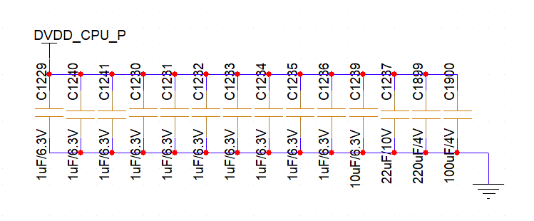
Place ten 1uF capacitors, one 10uF capacitor and one 22uF capacitor close to the DVDD_CPU_P pins. For DVDD_CPU_P, refer to the decoupling capacitor diagram below.
NPU Power
A210 chip's NPU power includes two parts: DVDD_NPU and DVDD_NPU_VIP.
| Power | Deepsleep | Vboot(V) | Supported Voltages(V) | Peak Current(mA) |
|---|---|---|---|---|
| DVDD_NPU | Not required to be powered | 0.8 | 0.75/0.8/0.9 | 2258.4 |
| DVDD_NPU_VIP | Not required to be powered | 0.8 | 0.75/0.8/0.9 | 13768.8 |
-
DVDD_NPU and DVDD_NPU_VI supports DVFS. These two power supply are combined in the reference design schematic.
-
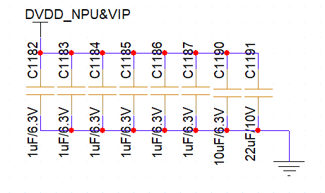
Place six 1uF capacitors, one 10uF capacitor and one 22uF capacitor close to the DVDD_NPU pins. For DVDD_NPU, refer to the decoupling capacitor diagram below.
-
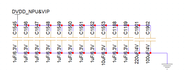
Place ten 1uF capacitors, one 10uF capacitor, one 100uF capacitor and one 220uF capacitor close to the DVDD_NPU_VIP pins. For DVDD_NPU_VIP, refer to the decoupling capacitor diagram below.
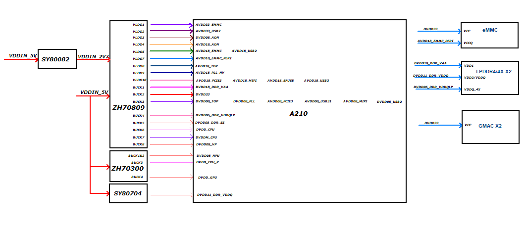
ZH70809G&ZH70300 Scheme Introduction
ZH70809G&ZH70300 Features
ZH70809G specifications are as follows.
| Package Size | Input Voltage | Standby Current | Type | Channel | Output Voltage Range | Voltage Regulation STEP | Voltage Accuracy (Static) | Transient Response (Dynamic) | Max Load Current (mA) | Communication |
|---|---|---|---|---|---|---|---|---|---|---|
| 4.21mm×4.21mm | 2.5V-5.5V | 20uA | Buck | BUCK1 | 1.2-3.5625 V | 37.5 mV | PWM Mode:±1% Normal Mode:±1.5% ECO Mode:±3% | VOUT:1.8V 0.5A/uS VPP:100mV | 1500 | I2C |
| BUCK2 | 1.7125-3.3 V | 12.5mV | PWM Mode:±1% Normal Mode:±1.5% ECO Mode:±3% | VOUT:2.5V 0.5A/uS VPP:100mV | 2000 | |||||
| BUCK3 | 0.7125-1.5V | 12.5 mV | PWM Mode:±1% Normal Mode:±1.5% ECO Mode:±3% | VOUT:1.1V 0.5A/uS VPP:60mV | 4000 | |||||
| BUCK4 | 0.3-1.0875V | 12.5mV | PWM Mode:±1% Normal Mode:±1.5% ECO Mode:±3% | VOUT:0.6V 0.5A/uS VPP:60mV | 1500 | |||||
| BUCK5/6 | 0.6-2.1875V | 12.5mV | PWM Mode:±1% Normal Mode:±2% ECO Mode:±3% | VOUT:1V 1A/uS VPP:40/50mV | 3000/4000 | |||||
| BUCK7 | 0.6-2.1875V | 12.5mV | PWM Mode:±1% Normal Mode:±2% ECO Mode:±3% | VOUT:0.9V 0.5A/uS VPP:100mV | 1000 | |||||
| BUCK8 | 0.6-2.1875V | 12.5mV | PWM Mode:±1% Normal Mode:±2% ECO Mode:±3% | VOUT:1.2V 0.5A/uS VPP:100mV | 1500 | |||||
| LDO | LDO1/2/5/7/10 | 1.2-3.3V | / | ±2% | VPP:100mV | 400 | ||||
| LDO4 | 0.6-3.3V | / | ±2% | VPP:100mV | 400 | |||||
| LDO3 | 0.6~1.15V | / | ±2% | VPP:100mV | 400 | |||||
| LDO8/9 | 0.75-1.8V | / | ±2% | VPP:100mV | 300 |
-
Supports programmable power-on sequencing.
-
6 additional GPIOs controllable via the I2C interface.
ZH70300 specifications are as follows.
| Package Size | Input Voltage | Standby Current | Type | Channel | Output Voltage Range | Voltage Regulation STEP | Voltage Accuracy (Static) | Transient Response (Dynamic) | Max Load Current (mA) |
|---|---|---|---|---|---|---|---|---|---|
| 2.66mm*3.84mm | 2.5V-5.5V | 6uA | Buck | BUCK1&BUCK2 | 0.3~1.85V | 5mV&10mV | ±1.25% | 12000 | |
| BUCK3 | 0.45-2V | 5mV&10mV | ±1.25% | 6000 | |||||
| BUCK4 | 0.45-2V | 5mV&10mV | ±1.25% | 6000 |
ZH70809G Considerations
-
ZH70809G VIO(PIN F5): Provides power to the internal digital logic. In the reference design schematic, VIO is powered by the ZH70809G’s LDO4 (1.8V). Notice that the high/low logic levels of the GPIO outputs are independent of the VIO voltage level.
-
ZH70809G RSTO(PIN C5): Outputs the reset signal to the SOC. Requires an external pull-up resistor to VIO. This signal will be driven High with a 40ms delay after all power rails have stabilized.
-
ZH70809G RSTI(PIN D6): The Reset Input for the ZH70809G. When this pin is triggered, all power rails will revert to their default voltage values, and RSTO will be output again. Notice that power rails configured as "Always-On" by default will not undergo a power cycle (they will not power on and off again).
-
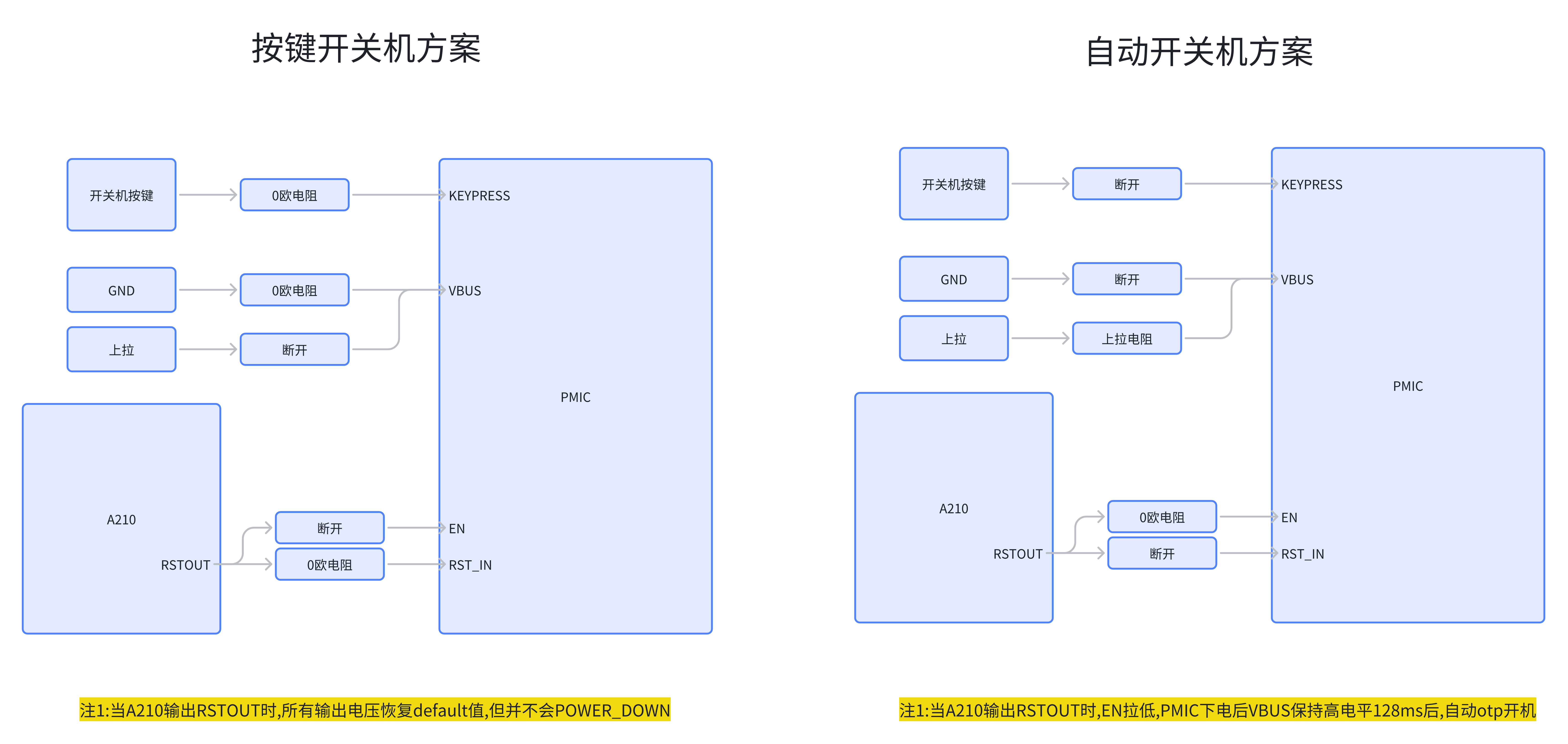
KZH70809G EYPRESS(PIN E8), EN(PIN C7), VBUS(PIN J5): These pins manage the ZH70809G power-on sequence. There are two mutually exclusive power-on/off schemes (refer to the diagram below):
- Manual Power-on/off Scheme: The system powers on after KEYPRESS is held Low for 4ms. Before powering off, KEYPRESS must be held Low for at least 1s (configurable up to 10s).
- Auto Power-on/off Scheme: When the A210's exception output pulls the EN pin Low, the system powers off and then automatically restarts after a 128ms delay.
-
ZH70809G SDA(PIN E4) SCL(PIN F4): I2C communication pins, must be pulled up to VIO.
-
For all other power input and output pins, please do not change the FB/SW trace, the input/output capacitor quantity and the inductor values at will. Refer to the schematic below.
ZH70300 Considerations
-
ZH70300 EN(PIN 1D): The power-on signal for the ZH70300, controlled by a ZH70809G GPIO.
-
ZH70300 SDA(PIN 2D) SCL(PIN 1C): I2C communication pins, must be pulled up to VIO.
-
ZH70809G VIO(PIN 3F): Provides power to the internal digital logic for the ZH70300. In the reference design schematic, VIO is powered by the ZH70809G's LDO4 (1.8V).
-
For all other power input and output pins, please follow these guidelines and refer to the schematic below.
- FB must use pseudo-differential routing. The reference design supports both local and remote sensing (Kelvin sensing).
- SW races must be kept short and wide.
- please do not change the input/output capacitor quantity and the inductor values at will.
A210 PMIC Power Supply Scheme
A210+ZH70809G+ZH70300+Independent BUCK POWER TREE
POWER TREE is as follows.
ZH70809G Power-On Sequence
The power-on sequence inside ZH70809G is fixed and cannot be replaced with other models. All EX-BUCK are all controlled by ZH70209GPIO。
A210+ZH70809G power-on sequence table is as follows.
| Power Name | PMIC Channel | Supply Limit(mA) | Time Slot | Default Voltage | Default ON/OFF |
|---|---|---|---|---|---|
| P3V3 | SY70209-BUCK2 | 2000 | 0 | 3.3 | ON |
| P2V7 | EX-BUCK | 2000 | 0 | 2.7 | ON |
| AVDD18_AON | SY70209-LDO4 | 400 | 1 | 1.8 | ON |
| DVDD08_AON | SY70209-LDO3 | 400 | 2 | 0.8 | ON |
| AVDD18_TOP | SY70209-LDO8 | 300 | 3 | 1.8 | ON |
| AVDD18_PERI1 | |||||
| AVDD18_PERI2 | |||||
| AVDD18_PLL | SY70209-LDO9 | 300 | 4 | 1.8 | ON |
| DVDD08_TOP | SY70209-BUCK3 | 4000 | 5 | 0.8 | ON |
| DVDD08_USB2 | |||||
| DVDD08_PLL | |||||
| AVDD08_USB31 | |||||
| AVDD08_MIPI | |||||
| AVDD08_PCIE | |||||
| AVDD18_EMMC | SY70209-LDO5 | 400 | 6 | 1.8 | ON |
| AVDD18_USB2 | |||||
| AVDD18_EMMC_PERI | SY70209-LDO7 | 400 | 7 | 1.8 | ON |
| AVDD18_FLASH_PERI | |||||
| AVDD33_EMMC | SY70209-LDO1 | 400 | 8 | 3.3 | ON |
| AVDD33_USB2 | SY70209-LDO2 | 400 | 9 | 3.3 | ON |
| DVDD08_DDR | SY70209-BUCK5 | 3000 | 10 | 0.8 | ON |
| DVDD11_DDR_VDDQ | EX-BUCK | 4000 | 11 | 1.1 | ON |
| DVDD06_DDR_VDDQLP | SY70209-BUCK4 | 1500 | 12 | 0.6 | ON |
| DVDD18_DDR_VAA | SY70209-BUCK1 | 1500 | 13 | 1.8 | ON |
| DVDD_CPU | SY70209-BUCK6 | 4000 | 14 | 0.8 | ON |
| DVDDM_CPU | SY70209-BUCK7 | 1000 | 15 | 0.8 | ON |
| AVDD18_EFUSE | SY70209-LDO10 | 400 | 16 | 1.8 | ON |
| AVDD18_PCIE3 | |||||
| AVDD18_USB3 | |||||
| AVDD18_MIPI |
Power consumption
The following data represents the peak currents of each core module during operation, provided for evaluating power schemes and PCB layout.
Caution:
The peak currents of individual modules cannot simply be summed up as the SoC's peak current. To assess thermal solutions, evaluate the average current consumption based on actual operating scenarios.
| Power Name | Voltage(V) | Current(mA) |
|---|---|---|
| P3V3 | 3.3 | 1500 |
| P2V7 | 2.7 | 1500 |
| AVDD18_AON | 1.8 | 50 |
| DVDD08_AON | 0.8 | 100 |
| AVDD18_TOP | 1.8 | 300 |
| AVDD18_PERI1 | ||
| AVDD18_PERI2 | ||
| AVDD18_PLL | 1.8 | 90.27 |
| DVDD08_TOP | 0.8 | 3244.84 |
| DVDD08_USB2 | ||
| DVDD08_PLL | ||
| AVDD08_USB31 | ||
| AVDD08_MIPI | ||
| AVDD08_PCIE | ||
| AVDD18_EMMC | 1.8 | 381.98 |
| AVDD18_USB2 | ||
| AVDD18_EMMC_PERI | 1.8 | 300 |
| AVDD18_FLASH_PERI | ||
| AVDD33_EMMC | 3.3 | 31.36 |
| AVDD33_USB2 | 3.3 | 10.53 |
| DVDD08_DDR | 0.8 | 2193 |
| DVDD_CPU | 1 | 3522.68 |
| DVDDM_CPU | 1 | 300 |
| AVDD18_MIPI | 1.8 | 281.24 |
| AVDD18_USB31 | ||
| AVDD18_EFUSE | ||
| AVDD18_PCIE | ||
| AVDD18_D2D | ||
| DVDD_NPU | 1 | 2258.4 |
| DVDD_NPU_VIP | 1 | 13768.8 |
| DVDD_VP | 1 | 1500 |
| DVDD_GPU | 1 | 1419 |
| DVDD_CPU_P | 1 | 5547.9 |
| DVDD08_D2D | 0.8 | 2796.63 |
| AVDD08_D2D | ||
| AVDD18_DDR_VAA | 1.8 | 167.94 |
| AVDD18_DDR_VDD1 | ||
| DVDD12_DDR_VDDQ | 1.1 | 2017.28 |
| DVDD12_DDR_VDD2 | ||
| DVDD06_DDR_VDDQLP | 0.6 | 1250 |
| DVDD06_DDR_VDDQ |
Functional Interface Design Guidelines
ADC Circuit
Overview
A210 integrates a 10-bit (configurable to 6-/8-10-bit) SAR ADC controller with a maximum sample rate of 2.5MSPS and an input voltage range of 0 to 1.8V. The specific pin assignments for the ADC are shown in the figure below.
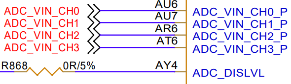
- Provides 4 channels (CH0 to CH3) of ADC input.
- ADC_DISLVL is the ADC control signal. In normal operation mode, the signal must be pulled down. Pull this signal up to avoid current consumption on analog power domain when entering Deepsleep mode or during the phase that AVDD18 is active but DVDD08_TOP has not yet stabilized.
Considerations
- The decoupling capacitor for ADC power supply must not be reduced. During layout, it should be placed close to the A210 pins.
- ADC_VIN_CH[3:0] are in use, and a 1nF capacitor must be added near the pins for debouncing.
USB2.0/USB3.1 Circuit
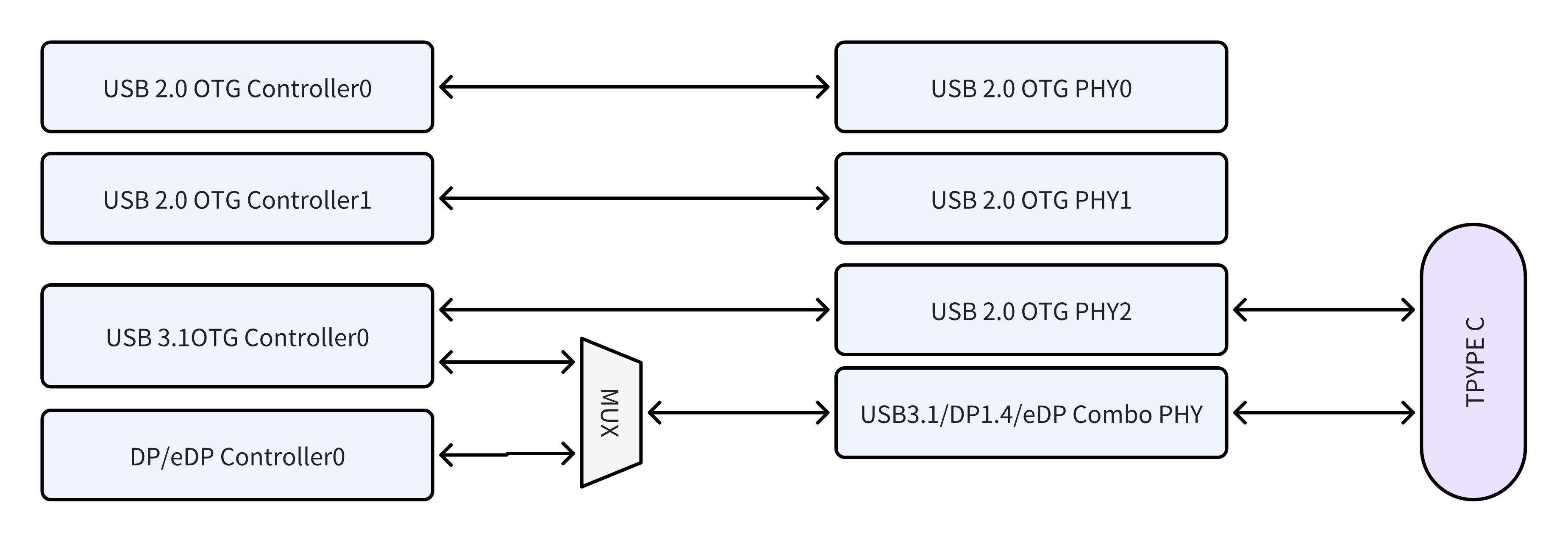
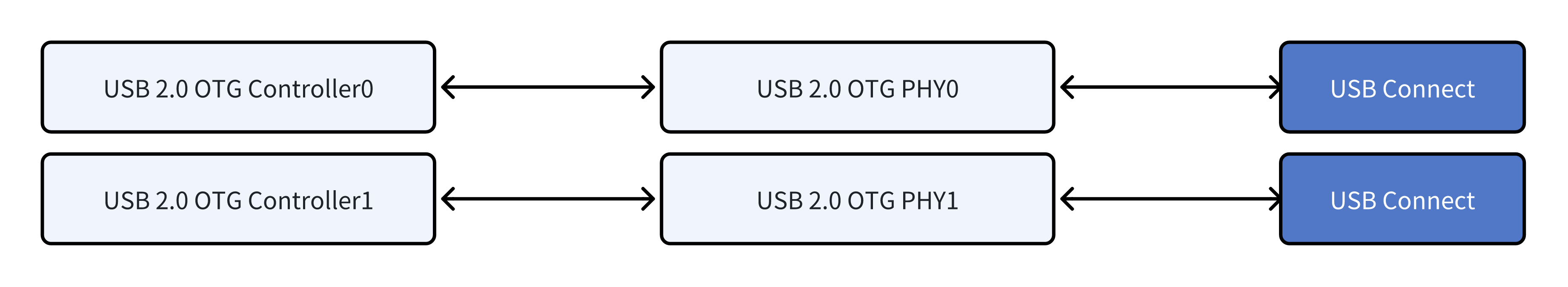
The A210 chip has one built-in USB3.1 controller and two built-in USB2.0 controllers.
The internal multiplexing diagram of the controller and PHY is as follows.
USB2.0 Circuit
Overview
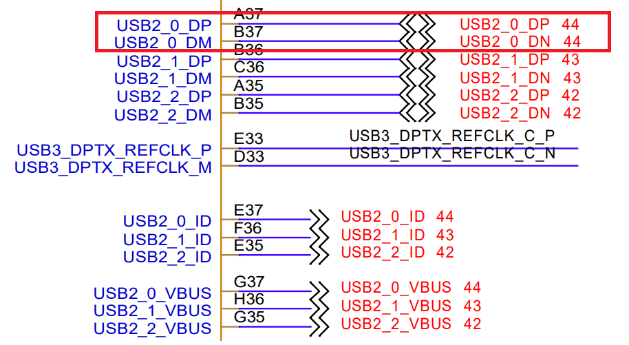
The A210 supports dual USB 2.0 interfaces. The detailed signals
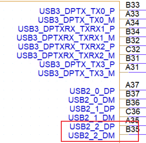
The USB2_0 signals are listed within the red box in the figure below.
The A210 supports flashing via USB2_0, which can be figured in BOOT_SEL[2:0]. The detailed configuration is as shown in the table below.
| BOOT_SEL[2] | BOOT_SEL[1] | BOOT_SEL[0] | BOOT MODE |
|---|---|---|---|
| 0 | 0 | 0 | USB Fastboot (Detect CCTboot first. Auto enter USB Fastboot if a 1-second timeout occurs) |
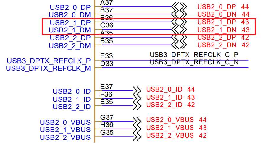
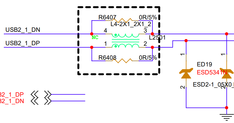
The USB2_1 signals are listed within the red box in the figure below.
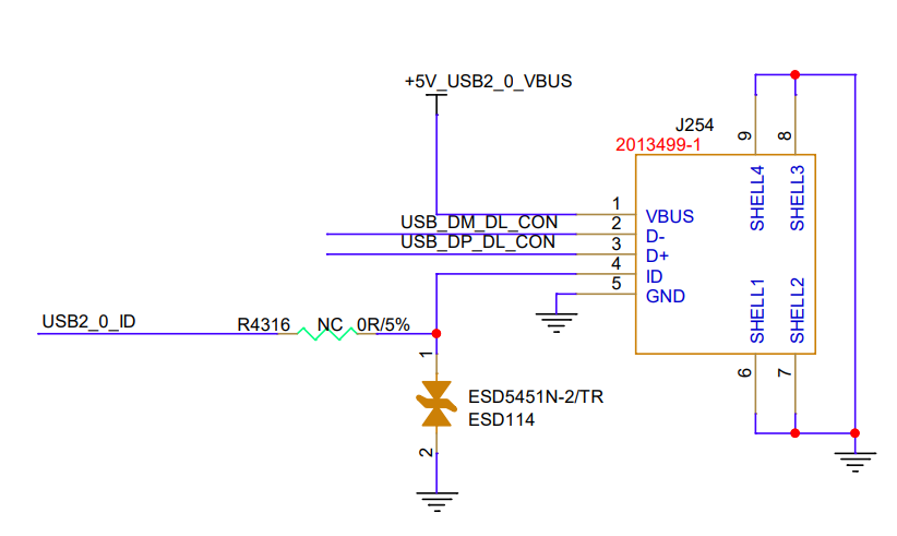
The two USB2.0 interface can be connected to USB connectors. The connection diagram is shown below.
Features
-
Both two USB2.0 interfaces support OTG. There are three modes can be configured.
-
OTG Mode: The system switches between Device and Host modes by identifying the state of the USB2_x_ID pin. Pull up to switch to the Device Mode. Pull down to switch to the Host Mode.
-
Device Mode: The USB2_x_ID pin is not required. The system only monitors the USB2_x_VBUS pin. When it is High, the DP line is pulled up to initiate enumeration.
-
HOST Mode: Neither the ID nor the VBUS status is required for operation in this mode.
Caution: The USB2_x_ID pin operates in the 1.8V power supply domain. USB2_x_VBUS operates in the 3.3V power supply domain.
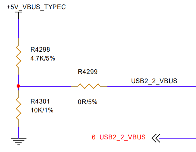
VBUS circuit is as shown in the diagram below.
-
-
Supports wake-up function.
-
To maintain high USB performance, the decoupling capacitor for PHY power supplies must not be reduced. During layout, they should be placed close to the pins.
-
ESD and surge resistance enhancement
-
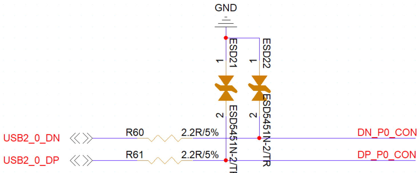
ESD devices must be reserved on all signals, and the parasitic capacitance of ESD for USB2.0 signals should not exceed 3pF.
Additionally, DP/DM for USB2.0 signals should be connected with a 2.2ohm resistor, as shown in the diagram below.
-
If USB2_x_ID is used, both ESD devices and a series resistor must be reserved on signals. USB2_x_ID pin circuit is as shown in the diagram below.
-
-
To suppress electromagnetic radiation, consider reserving common mode chokes (common mode choke) on signal lines. Depending on the actual situation, resistors or common mode chokes can be used during debugging. The USB2.0 signal series connect to 2.2ohm resistor is shown in the diagram below.
Recommendations
The following table shows the recommended matching design for USB2.0 ports.
| Signal | Connection Method | Description |
|---|---|---|
| USB2_0P | Serial connection with 2.2ohm resistor | USB2_0 USB signal, data input/output |
| USB2_0M | Serial connection with 2.2ohm resistor | |
| USB2_0_ID | USB OTG ID detection with a power supply domain of 1.8 | |
| USB2_0_VBUS | Voltage divider detection | USB OTG insertion detection |
| USB2_1P | Serial connection with 2.2ohm resistor | USB2_1 USB signal, data input/output |
| USB2_1M | Serial connection with 2.2ohm resistor | |
| USB2_1_ID | USB OTG ID detection with a power supply domain of 1.8 | |
| USB2_1_VBUS | Voltage divider detection | USB OTG insertion detection |
USB3.1/DP/eDP Circuit
Overview
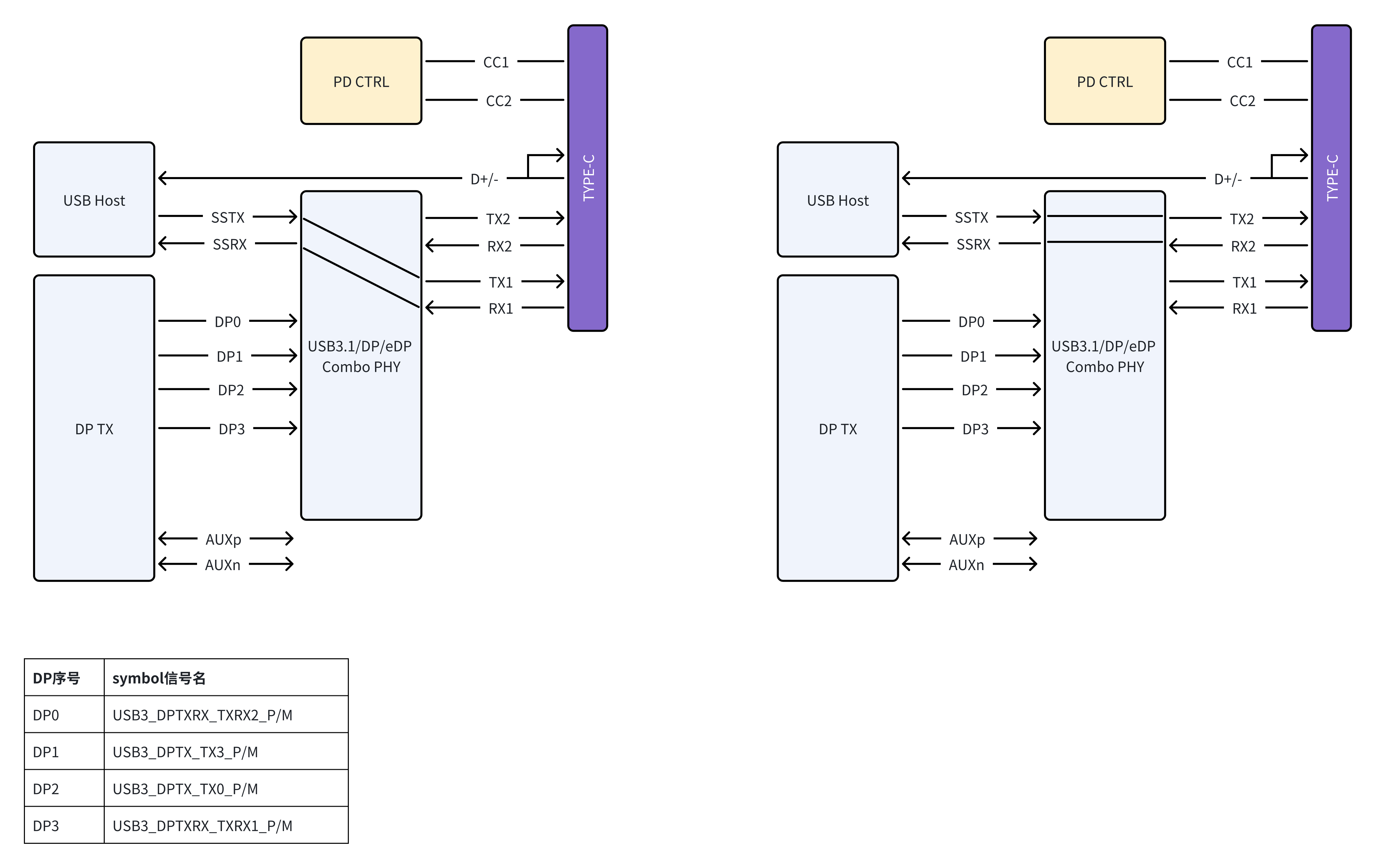
USB3.1 controller supports both Host and Device mode, backward compatible with USB 2.0 and USB 1.1.
The USB2.0 signal names are listed within the red box in the figure below.
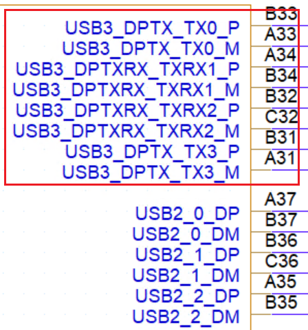
The USB3.1 SS signals (10Gbps) are multiplexed with DP/eDP, using a USB/DP/eDP Combo PHY。The USB3.1 signal names are listed within the red box in the figure below.
The USB3.0 Controller0 and DP1.4 Controller0 combined with the USB3.0/DP1.4 Combo PHY0 form a complete Type-C port.
This USB3.1/DP1.4/eDP Combo PHY supports Lane swapping (SWAP), enabling the following five possible configurations in actual implement.
Note:
The simplified connection diagrams are shown below. Additional AC coupling capacitors, pull-up resistors, and USB protection circuits are not depicted. Please refer to the EVB schematics for detailed information.
-
USB3.1 Only => Type-C "Normal" & "Flip"
-
USB3.1 + 2 Lane DP1.4 => Type-C (Normal - Flip shown‘dashed’)
-
USB2.0 + 4 Lane DP1.4 => Type-C (Normal - Flip shown‘dashed’)
-
USB3.1(Only) +2 Lane DP/eDP
The model enables flexible allocation of high-speed interface resources and maximize the utilization efficiency of the pins.
Caution:
This specific configuration does not natively support the Type-C connector logic. An external analog switch or MUX is required if enabling Type-C functionality.
-
USB2.0 Only => Type-C + 4 Lane DP/eDP
The model enables flexible allocation of high-speed interface resources and maximize the utilization efficiency of the pins.
Features
-
Since USB3.1 OTG and USB2_2 OTG share the same USB3.1 controller, USB3.1 and USB2_2 OTG can only function simultaneously as Device or HOST.
Caution: The following USB OTC mode combinations cannot be implemented.
- USB3.1 OTG to be HOST while USB2_2 OTG acts as Device.
- USB3.1 OTG to be Device while USB2_2 OTG acts as HOST.
-
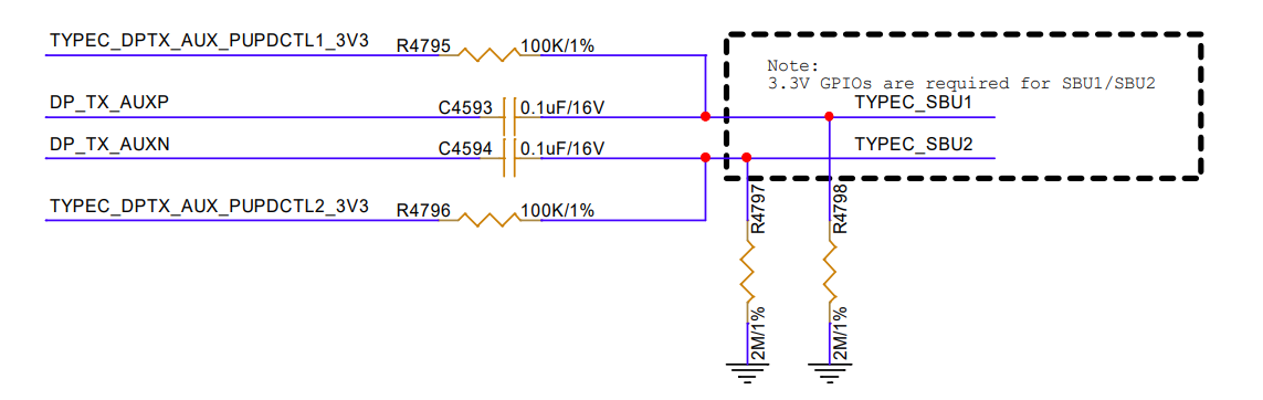
The DPTX_AUX_P/N pins in DP ALT interface are used to transmit AUX signals, enabling the USB3.1/DP AUX PHY functionality. The pin definitions for the AUX signals are as follows.

100nF capacitors are connected in series to the Type-C SU1/2 pin, with a 100kΩ resistor (one pulled up to 3.3V, one pulled down to GND) connected to each line separately. It is recommended to use two 3.3V GPIO to these two 100kΩ resistors, switching between 3.3V and GND based on the orientation detected by CC/PD controller (control signal from the PD controller). When the USB3.1/DP AUX PHY is used as UFP_D, the two resistors to be driven on the board are 1MΩ. The AUX reference circuit is as follows.
-
All signals on the Type-C connector must have ESD protection devices placed close to the connector. For SSTXP/N and SSRXP/N lines, the parasitic capacitance of the ESD device must not exceed 0.3 pF.
Recommendations
The following table shows the recommended matching design for USB3.1/DP/eDP ports.
| Signal | Connection Method | Description |
|---|---|---|
| USB2_2P | Serial connection with 2.2ohm resistor | USB2.0 Signal, data input/output |
| USB2_2M | Serial connection with 2.2ohm resistor | |
| USB3_DPTX_TX0_P | Serial connection with 100nF capacitor | USB3.1 TX signal or DP/eDP TX signal |
| USB3_DPTX_TX0_M | Serial connection with 100nF capacitor | |
| USB3_DPTXRX_TXRX1_P | Serial connection with 0ohm resistor | USB3.1 RX signal or DP/eDP RX/TX signal |
| USB3_DPTXRX_TXRX1_M | Serial connection with 0ohm resistor | |
| USB3_DPTXRX_TXRX2_P | Serial connection with 0ohm resistor | USB3.1 RX signal or DP/eDP RX/TX signal |
| USB3_DPTXRX_TXRX2_M | Serial connection with 0ohm resistor | |
| USB3_DPTX_TX3_P | Serial connection with 100nF capacitor | USB3.1 TX signal or DP/eDP TX signal |
| USB3_DPTX_TX3_M | Serial connection with 100nF capacitor | |
| USB_DPTX_REFCLK_P | Left floating | |
| USB_DPTX_REFCLK_M | ||
| DPTX_AUX_P | 100nF capacitors are connected in series to the Type-C SU1/2 pin, with a 100kΩ resistor tied to 3.3V I/Os, which switch between 3.3V and GND based on the orientation detected by the CC/PD controller. | In DP Alt Mode, connects to the Type-C SU1/2 pin to Perform operations such as video signal transmission and so on. |
| DPTX_AUX_N | ||
| USB2_2_ID | USB OTG ID detection. Operating voltage domain: 1.8V. | |
| USB2_2_VBUS | Voltage divider detection | USB OTG insertion detection |
SATA Circuit
Features
The A210 chip features 2 SATA3.0 controllers. The SATA3.0 features are as follows.
- Supports SATA PM function.
- Supports SATA 1.5Gb/s, SATA 3.0Gb/s and SATA 6.0Gb/s speeds.
- Supports wake-up function
Pin Definition/IO Multiplexing Relation
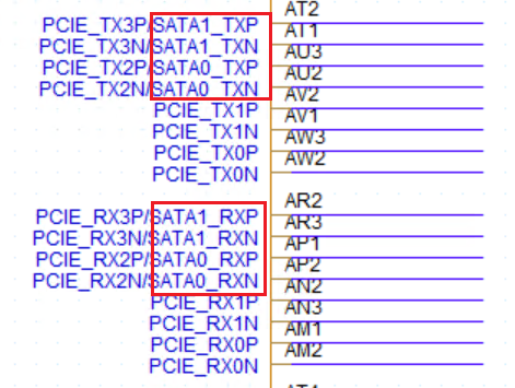
SATA3.0 and PCIE are multiplexed. The multiplexing relations are shown in the table below.
| PHY | PHY0(x2) | PHY1(x2) | ||
| lane# | 0 | 1 | 2 | 3 |
| NO. | Configuration | |||
| 1 | PCIE x4 (PCIE DM) | |||
| 2 | PCIE x2(PCIE_DM) | PCIE x1(PCIE_RP) | N/A | |
| 3 | PCIE x2(PCIE_RP) | x2(SATA) | ||
| 4 | PCIE x1(PCIE_DM) | PCIE x1(PCIE_RP) | x2(SATA) | |
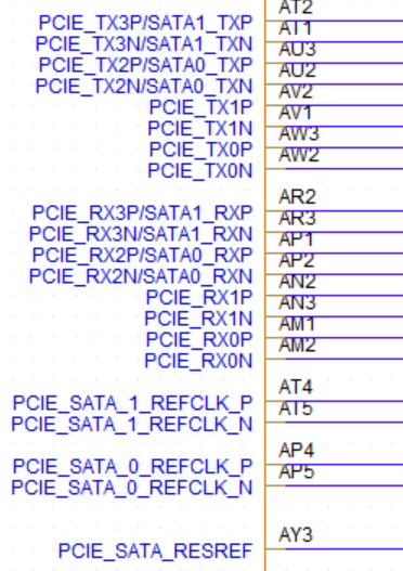
The related pin definitions of SATA0 and SATA1 are as follows.
Related control IOs for SATA0/1 controllers include.
Caution: The controls are implemented via I/O multiplexing. All IO power domains operate at 1.8V. Ensure proper level matching during design.
- SATA_Px_DEVSLP: SATAx device sleep control pin, enabling SSDs to enter or exit low-power consumption states through ts high and low voltage levels.
- SATA_Px_MP_SWITCH: Input for switch detection of SATAx hot-plug devices.
- SATA_Px_CP_DET: Input for hot-plug detection of SATAx devices.
- SATA_Px_CP_POD: Output for power switch control of SATAx hot-plug devices.
- SATA_Px_ACT_LED: Controls LED blinking when data is transferred through the SATAx interface.
Recommendations
Considerations for SATA design:
- When designing slots, peripheral circuits and power supplies must meet Spec requirements.
- For SATA interface TXP/N, RXP/N, 10nF AC coupling capacitors are serially connected, AC coupling capacitors are recommended to use 0201 package for lower ESR and ESL, which can also reduce impedance changes on the line.
- All signals of the eSATA interface socket must have ESD devices added, placed near the socket during layout, and the parasitic capacitance of ESD should not exceed 0.4pF.
SATA interface design recommendations are as follows.
| Signal | Connection Method | Description |
|---|---|---|
| PCIE_RX2N/SATA0_RXN | Serial connection with 10nF capacitor | SATA0 data input |
| PCIE_RX2P/SATA0_RXP | Serial connection with 10nF capacitor | SATA0 data input |
| PCIE_TX2N/SATA0_TXN | Serial connection with 10nF capacitor | SATA0 data output |
| PCIE_TX2P/SATA0_TXP | Serial connection with 10nF capacitor | SATA0 data output |
| PCIE_SATA_0_REFCLK_P/M | 100M clock | SATA0 reference clock |
| PCIE_RX3N/SATA1_RXN | Serial connection with 10nF capacitor | SATA1 data input |
| PCIE_RX3P/SATA1_RXP | Serial connection with 10nF capacitor | SATA1 data input |
| PCIE_TX3N/SATA1_TXN | Serial connection with 10nF capacitor | SATA1 data output |
| PCIE_TX3P/SATA1_TXP | Serial connection with 10nF capacitor | SATA1 data output |
| PCIE_SATA_1_REFCLK_P/M | 100M clock | SATA1 reference clock |
PCIe Circuit
Configuration
A210 has two (2-lane) PCIe 2.1 controllers, supporting PCIe 3.1/2.1/1.1.
PCIE PHY are combined with SATA PHY, enabling the following four configurations(DM: Dual Mode,RP: Root Port).
| PHY | PHY0(x2) | PHY1(x2) | ||
| lane# | 0 | 1 | 2 | 3 |
| NO. | Configuration | |||
| 1 | PCIE x4 (PCIE DM) | |||
| 2 | PCIE x2(PCIE_DM) | PCIE x1(PCIE_RP) | N/A | |
| 3 | PCIE x2(PCIE_RP) | x2(SATA) | ||
| 4 | PCIE x1(PCIE_DM) | PCIE x1(PCIE_RP) | x2(SATA) | |
- Two 2lane PCIE3.0 PHY forms PCIe 3.0 x4 DM mode.
- One 2lane PCIE3.0 DM mode + One PCIe 3.0 x1 RP mode.
- One 2lane PCIE3.0 DM mode + Two SATA.
- One PCIe 3.0 x1 DM mode + One PCIe 3.0 x1 RP mode + Two SATA.
Pin Definition
PCIEX4_TYPE pin to select PCIE mode.
![]()
The PCIe interface design recommendations are as follows.
| Signal | Function Description | Recommendations |
|---|---|---|
| PCIEX4_TYPE | PCIE TYPE Selection: 0: EP. 1: RC. | Select as needed. |
The pin information for PCIe-related signals is shown in the figure below.
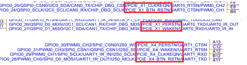
Additionally, PCIe includes four sideband signals: BTN_RSTN, CLKREQN, PERSTN, and WAKE, all of which are implemented via GPIO multiplexing. As shown in the figure below, the power domain for these I/O pins is 1.8V.
PCIe-related pin information and interface design recommendations are as follows.
| Signal | Connection Method | Description |
|---|---|---|
| PCIE_TX0/1N/P | Serial connection with 100nF capacitor | PCIe data output |
| PCIE_RX0/1N/P | Direct connection | PCIe data input |
| PCIE_TX2/3N/P | Serial connection with 100nF capacitor | PCIe data output. Data output as SATA0/1 in SATA mode |
| PCIE_RX2/3N/P | Direct connection | PCIe data output. Data output as SATA0/1 in SATA mode |
| PCIE_SATA_0_REFCLK_P/M | 100M clock | PCIe0 reference clock |
| PCIE_SATA_1_REFCLK_P/M | 100M clock | PCIe1 reference clock |
| PCIE_SATA_RESREF | 200ohm to GND | External reference resistor pin |
| PCIE_X1/4_CLKREQN | Serial connection with 0ohm resistor. IO power domain operates at 1.8V. Ensure proper level matching during design. Add level conversion circuits add needed | PCIe reference clock request output |
| PCIE_X1/4_PERSTN | Serial connection with 0ohm resistor. IO power domain operates at 1.8V. Ensure proper level matching during design. Add level conversion circuits add needed | PCIe global reset output (RC mode)/PCIe global reset input (X4 EP mode) |
| PCIE_X1/4_WAKEN | Serial connection with 0ohm resistor. IO power domain operates at 1.8V. Ensure proper level matching during design. Add level conversion circuits add needed | PCIe wake-up output (EP mode) |
| PCIE_X1/4_BTN_RSTN | Reserved | External physical reset pin of PCIe Controller. Active low. Pulled down PCIe to reset |
Recommendations
Considerations for PCIe design:
-
When designing slots, peripheral circuits, and power supplies, they must meet Spec requirements.
-
For PCIe interface, 220nF AC coupling capacitors are serially connected to TXP/N differential signals. AC coupling capacitors are recommended to use 0201 package for lower ESR and ESL, which can also reduce impedance changes on the line.
-
PCIE_X4_BTN_RSTN, PCIE_X4_CLKREQN, PCIE_X4_PERSTN, PCIE_X4_WAKE, PCIE_X1_BTN_RSTN, PCIE_X1_CLKREQN, PCIE_X1_PERSTN and PCIE_X1_WAKE are all at 1.8V level. Attention should be paid to proper level matching. The level conversion circuits required when interfacing with other levels.
-
When PCIe operates in RC mode, the CLKREQ signal functions as an output and is normally pulled low during normal operation to provide the clock for PCIe_SATA_0/1_REFCLK. Simultaneously, when an EP device pulls CLKREQ_EP low, it indicates a request for the PCIe reference clock from the RC. This requires supplying a 100MHz clock to the EP device. Refer to the diagram below.
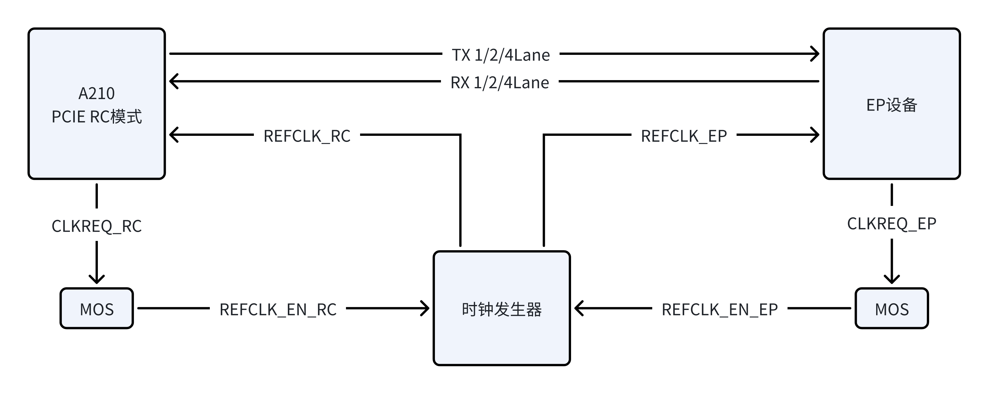
-
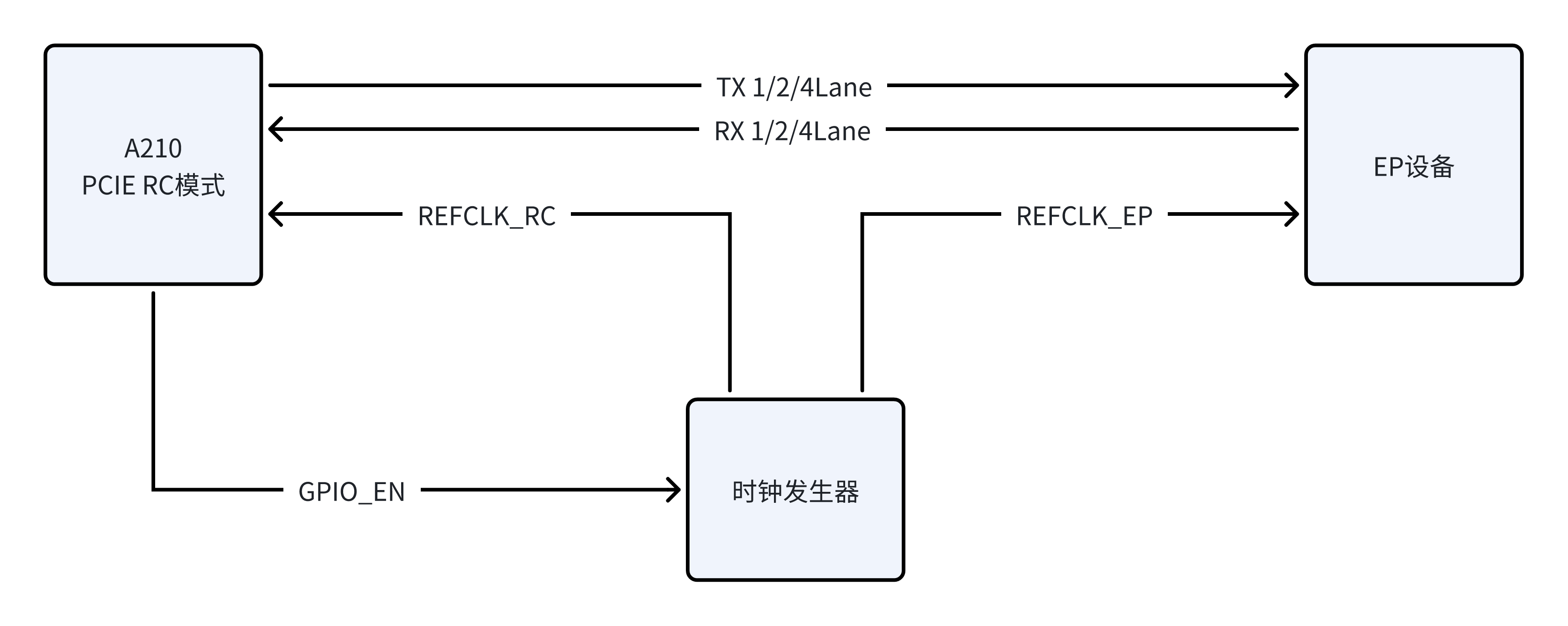
If cost is a consideration, the CLKREQN signal can also be left unconnected. Use a standard GPIO as the clock generator enable pin. After system startup, it directly controls the clock output. See the following reference:
-
When PCIe operates in EP mode, the CLKREQ signal initially functions as an output to request the PCIe reference clock. Pulling it low requests a clock from the RC device.
-
The PERST signal is the PCIe global reset signal, active low, serving as the PCIe global reset. When this signal is asserted, the EP device resets its internal logic to a known state
-
WAKEN is a wake-up signal active only in EP mode, functioning as an output with low-active logic. It is primarily used to submit wake-up requests to the RC after the EP has entered the low-power sleep mode. WAKEN is an optional signal. When operating in RC mode, an AON pin can be selected as the wake-up I/O to utilize the WAKEN functionality.
-
BTN_RSTN is an external physical reset pin with low-active logic. Recommended to reserve.
Video Input Interface Circuit
MIPI DPHY CSI Interface
Overview
A210 has two MIPI DPHY CSI RX interface, both support MIPI V1.2. The maximum transmission rate per channel is 2.5Gbps.
- Supports 4x2lane, 2x4lane and 1x4lane + 2x2lane mode.
- Supports 8/10/12/16-bit widths.
- Supports 4-lane 1080P@30fps, 1x4K@30fps, 2x1080P@60fps input.
- Supports a maximum input resolution of 12M Pixel。
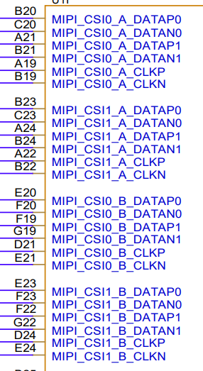
MIPI DPHY CSI0 RX interface supported modes are as follows.
-
Supports x4Lane mode, MIPI_CSI0_A/B_DATA0[1:0] data refer to MIPI_CSI0_A_CLK.
-
Supports x2Lane + x2Lane mode.
- MIPI_CSI0_A_DATA0[1:0] data refer to MIPI_CSI0_A_CLK.
- MIPI_CSI0_B_DATA0[1:0] data refer to MIPI_CSI0_B_CLK.
CSI0 RX interface's Lane and CLK assignments for each mode are shown in the table below.
| Option1 | sensor1 x4 Lane | MIPI_CSIO_A_DATA0/1 MIPI_CSIO_B_DATA0/1 MIPI_CSIO_A_CLK |
| Option2 | sensor1 x2 Lane | MIPI_CSI1_A_DATA0/1 MIPI_CSI1_A_CLK |
| sensor2 x2 Lane | MIPI_CSI1_B_DATA0/1 MIPI_CSI1_B_CLK |
MIPI DPHY CSI1 RX interface supported modes are as follows.
-
Supports x4Lane mode, MIPI_CSI1_A/B_DATA0[1:0] data refer to MIPI_CSI1_A_CLK.
-
Supports x2Lane + x2Lane mode
- MIPI_CSI1_A_DATA0[1:0], data refer to MIPI_CSI1_A_CLK.
- MIPI_CSI1_B_DATA0[1:0], data refer to MIPI_CSI1_B_CLK.
CSI0 RX interface's Lane and CLK assignments for each mode are shown in the table below.
| Option1 | sensor1 x4 Lane | MIPI_CSI1_A_DATA0/1 MIPI_CSI1_B_DATA0/1 MIPI_CSI1_A_CLK |
| Option2 | sensor1 x2 Lane | MIPI_CSI1_A_DATA0/1 MIPI_CSI1_A_CLK |
| sensor2 x2 Lane | MIPI_CSI1_B_DATA0/1 MIPI_CSI1_B_CLK |
Recommendations
MIPI CSI0/1 RX design note:
- In order to improve the MIPI CSI0/1 RX performance, the decoupling capacitors of each power supply of the PHY should not be removed, and please place them close to the pins in the layout (Included power: DVDD08_TOP, AVDD08_MIPI and AVDD18_MIPI).
- For board-to-board (BTB) connector interfaces, it is recommended to reserve TVS diodes.
MIPI DPHY CSI0/1 RX matching design recommendations are shown in the table below.
| Signal | Connection Method | Description |
|---|---|---|
| MIPI_CSI0_A_DATAP/N0 | Direct connection | MIPI CSI0 data Lane0 input |
| MIPI_CSI0_A_DATAP/N1 | Direct connection | MIPI CSI0 data Lane1 input |
| MIPI_SCI0_A_CLKP/N | Direct connection | MIPI CSI0 clock 0 input |
| MIPI_CSI0_B_DATAP/N0 | Direct connection | MIPI CSI0 data Lane2 input |
| MIPI_CSI0_B_DATAP/N0 | Direct connection | MIPI CSI0 data Lane3 input |
| MIPI_SCI0_B_CLKP/N | Direct connection | MIPI CSI0 clock 1 input |
| MIPI_CSI1_A_DATAP/N0 | Direct connection | MIPI CSI1 data Lane0 input |
| MIPI_CSI1_A_DATAP/N0 | Direct connection | MIPI CSI1 data Lane1 input |
| MIPI_SCI1_A_CLKP/N | Direct connection | MIPI CSI1 clock 0 input |
| MIPI_CSI1_B_DATAP/N0 | Direct connection | MIPI CSI1 data Lane2 input |
| MIPI_CSI1_B_DATAP/N0 | Direct connection | MIPI CSI1 data Lane3 input |
| MIPI_SCI1_B_CLKP/N | Direct connection | MIPI CSI1 clock 1 input |
Video Output Interface Circuit
MIPI DPHY DSI Interface
Overview
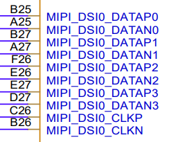
A210 has one 4Lane DSI TX, supporting MIPI V1.2 version. Maximum transfer rate is 2.5Gbps/Lane. Maximum resolution supports 4K@60fps.
Recommendations
MIPI DSI TX design note:
- In order to improve the MIPI DSI TX performance, the decoupling capacitors of each power supply of the PHY should not be removed, and please place them close to the pins in the layout (Included power: DVDD08_TOP, AVDD08_MIPI and AVDD18_MIPI).
- For board-to-board (BTB) connector interfaces, it is recommended to reserve TVS diodes.
MIPI DPHY DSI TX matching design recommendations are shown in the table below.
| Signal | Connection Method | Description |
|---|---|---|
| MIPI_DSI0_DATAP/N0 | Direct connection | MIPI DSI data Lane0 output |
| MIPI_DSI0_DATAP/N1 | Direct connection | MIPI DSI data Lane1 output |
| MIPI_DSI0_DATAP/N2 | Direct connection | MIPI DSI data Lane2 output |
| MIPI_DSI0_DATAP/N3 | Direct connection | MIPI DSI data Lane3 output |
| MIPI_DSI0_CLKP/N | Direct connection | MIPI DSI clock output |
HDMI TX Interface
A210 has one HDMI TX PHY, supports HDMI2.0 version.
- Maximum resolution supports 4K@60fps.
- Supports HDCP 1.4.
- Supports audio output.
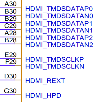
HDMI_HPD is the HPD pin. The power domain operates at 1.8V. Since the HPD high level voltage in the HDMI interface ranges from 2.0 to 5.3V, a level shifter circuit is required.
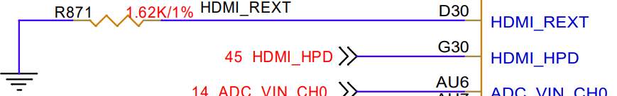
HDMI_REXT is the external reference resistor pin for HDMI PHY, external 1.62Kohm resistor with 1% accuracy to ground, the resistor value must not be changed, and the layout is placed close to the A210 chip pin.
HDMI includes HDMI_CEC, HDMI_SCL, HDMI_SDA and other auxiliary pins, which are multiplexed via GPIOs. The detailed HDMI signal auxiliary pins are shown in the figure below.
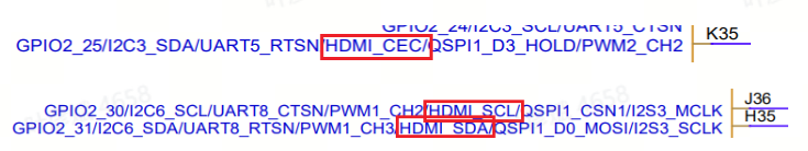
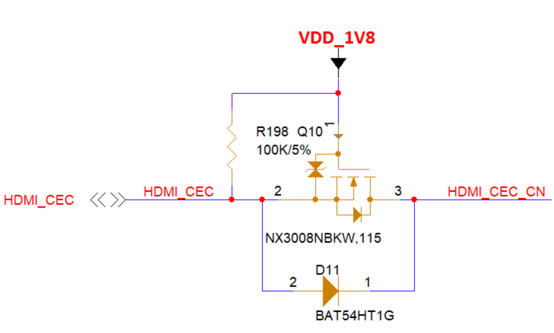
HDMI_CEC (voltage level of 1.8V) is the HDMI controller CEC function multiplexed to the ordinary GPIO function. The CEC protocol specifies a 3.3V level, but the protocol requires that 3.3V be applied to the CEC pin through a 27K resistor, and leakage is not allowed to exceed 1.8uA.
The A210 IO Domain will have leakage on the IO if there is voltage on the IO when it is not powered up. For example, A210 has been powered off, but the HDMI cable is still connected to the Sink side (TV or monitor), at this time there is power at the Sink side of the CEC, which will leak through the HDMI cable to the A210 IO, resulting in CEC leakage of more than 1.8uA, so it is necessary to add an external isolation circuit. CEC isolation circuit is shown in the figure below.
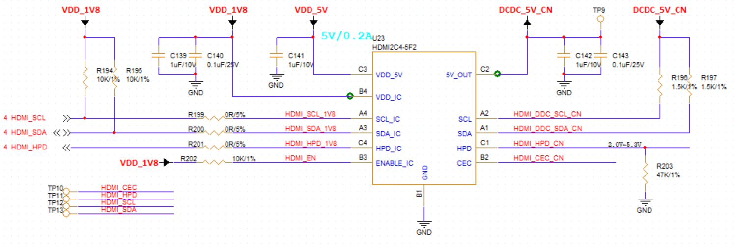
HDMI_SCL and HDMI_SDA are the I2C/DDC bus of the HDMI TX controllers. The protocol specifies a 5V level, so a level conversion circuit is required.
In the reference design schematic, HDMI2C-5F2 adopted by HDMI-related auxiliary signals implements level conversion and power control. HDMI auxiliary signal reference circuit is shown in the figure below.
In order to strengthen the anti-static ability, the signal must be reserved ESD devices, HDMI2.1 signal ESD parasitic capacitance shall not exceed 0.2pF, other signals ESD parasitic capacitance is recommended to use no more than 1pF.
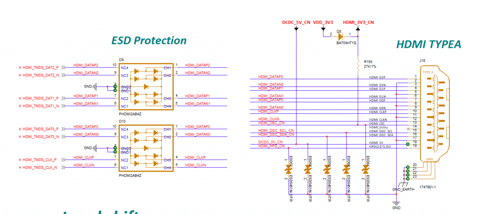
HDMI TX matching design recommendations are shown in the table below.
| Signal | Connection Method | Description |
|---|---|---|
| HDMI_TMDSDATAP/N0 | Direct connection | TMDS data Lane0 |
| HDMI_TMDSDATAP/N1 | Direct connection | TMDS data Lane1 |
| HDMI_TMDSDATAP/N2 | Direct connection | TMDS data Lane2 |
| HDMI_TMDSCLKP/N | Direct connection | TMDS clock |
| HDMI_REXT | 1.62Kohm with 1% accuracy resistor to ground | External reference resistor |
| HDMI_HPD | HDMI2C-5F2 conversion | HPD detection |
| HDMI_CEC | MOS isolation | CEC signal |
| HDMI_SCL | HDMI2C-5F2 conversion | DDC clock |
| HDMI_SDA | HDMI2C-5F2 conversion | DDC data input/output |
DP/eDP Interface
Overview
A210 supports one DP1.4/eDP1.5 TX PHY (combined with USB3.1), with a maximum resolution of 4K@60fps.
- Each Lane rate can support 1.62/2.7G/5.4/8.1Gbps.
- Supports 2Lane or 4Lane mode.
- Supports wake-up
- Supports audio output.
Recommendations
DP/eDP TX PHY design note.
- TX line need to be connected in series with 100nF AC coupling capacitors, AC coupling capacitors are recommended to use 0201 packages, lower ESR and ESL, and also reduces impedance changes on the line. Layout is placed close to the A210 pin.
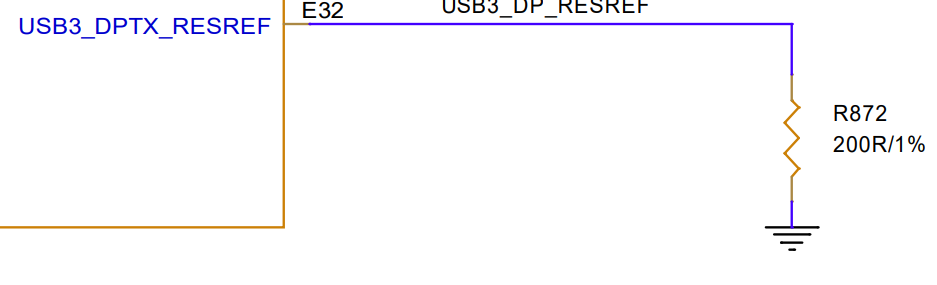
- USB3_DPTX_RESREF is the external reference resistor pin for USB DP Combo PHY, external 200ohm precision 1% resistor to ground, resistor value must not be changed, layout placed close to the A210 chip pin.
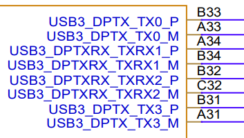
DP0/1 TX PHY interface matching design is as follows.
| Signal | Connection Method | Description |
|---|---|---|
| USB3_DPTX_TX0_P | Serial connection with 100nF capacitor | DP/eDP Lane0 output |
| USB3_DPTX_TX0_M | Serial connection with 100nF capacitor | |
| USB3_DPTXRX_TXRX1_P | Serial connection with 100nF capacitor | DP/eDP Lane1 output |
| USB3_DPTXRX_TXRX1_M | Serial connection with 100nF capacitor | |
| USB3_DPTXRX_TXRX2_P | Serial connection with 100nF capacitor | DP/eDP Lane2 output |
| USB3_DPTXRX_TXRX2_M | Serial connection with 100nF capacitor | |
| USB3_DPTX_TX3_P | Serial connection with 100nF capacitor | DP/eDP Lane3 output |
| USB3_DPTX_TX3_M | Serial connection with 100nF capacitor | |
| USB_DPTX_REFCLK_P | Left floating | |
| USB_DPTX_REFCLK_M | ||
| DPTX_AUX_P | 100nF capacitors are connected in series to the Type-C SU1/2 pin, with a 100kΩ resistor tied to 3.3V I/Os, which switch between 3.3V and GND based on the orientation detected by the CC/PD controller. | DP AUX channel |
| DPTX_AUX_N |
LCD Screen and Touch Screen Design Notes
- For the current limiting resistor on the FB side of the LED backlight boost IC, please choose 1% precision resistor and select the appropriate package size according to the power requirement.
- For the EN/PWM pin of the LED backlight boost IC, choose the GPIO with internal pull-down and external pull-down resistor to avoid the flashing screen phenomenon when powering up.
- LED backlight drive voltage output, please choose the appropriate rated voltage filter capacitor.
- For the Schottky diode of the LED backlight boost circuit, please choose the appropriate model according to the operating current and pay attention to the reverse breakdown voltage of the diode to avoid reverse breakdown at no load.
- For the inductor of LED backlight boost circuit, please match the inductance, saturation current, DCR, etc. according to the actual model.
- The signal level of the screen and touch screen should be matched with the IO driver level of the chip, such as RST/Stand by and other signals.
- The power supply of the screen must be controllable and not provided by default when powering up.
- The decoupling capacitors for the screen and touchscreen must not be deleted, they must be retained.
- The I2C bus of TP must add 2.2K pull-up to VCC3V3_TP power supply, it is recommended not to share the bus with other devices, if you must share, pay attention to the pull-up power supply and address conflict.
- For TP IC with Charge pump, please pay attention to the rated voltage of capacitor.
- For the screen, when connecting to the board via FPC, it is recommended to connect a resistor with a certain resistance value (between 22ohm-100ohm, subject to SI test), and reserve TVS devices.
- It is recommended to reserve common mode inductors at the interface for screens with serial interface.
Audio Circuit Design
A210 provides a total of 4 sets of I2S interfaces and 1 set of PDM interfaces.
I2S
Overview
A210 provides a total of 4 sets of I2S interfaces. As the most widely used digital audio interface, I2S can be used for communication between audio ADCs, audio DACs, audio codecs, DSPs, and other peripherals. It can also provide integrated audio input and output support for video input/output interfaces.
I2S3 is a standard I2S interface supporting 8-channel input/output capability, while I2S0, I2S1, and I2S2 are standard I2S interfaces supporting 2-channel input/output capability.
I2S3 features are as follows.
- Supports 8-channel input/output.
- Supports RX/TX full-duplex.
- Supports a maximum sampling rate of 384KHz.
- Supports master-slave mode.
- Supports sampling accuracy ranging from 16 to 32 bits.
- Supports three I2S formats (standard, left-aligned, right-aligned).
- PCM mode supports both standard and custom modes (frame sync signal only supports short pulse sync signals, with a sync signal duration of one clock cycle).
I2S0/1/2 features are as follows.
- Supports 2-channel input/output.
- Supports RX/TX full-duplex.
- Supports a maximum sampling rate of 384KHz.
- Supports master-slave mode.
- Supports sampling accuracy ranging from 16 to 32 bits.
The I2S interface output data lines (SDOx) and input data (SDIx), use the same set of bit/frame (SCLK/WS) reference clocks.
Recommendations
I2S IO assignments and design recommendations are as follows.
| Signal | Power Domain | Connection Method | Description |
|---|---|---|---|
| I2S0_MCLK | AVDD18_PERI1 | Serial connection with 22ohm resistor | I2S system clock output |
| I2S0_SCLK | Serial connection with 22ohm resistor | I2S continuous serial clock, bit clock | |
| I2S0_WS | Serial connection with 22ohm resistor | I2S frame clock for channel selection | |
| I2S0_SDI | Serial connection with 22ohm resistor | I2S serial data 0 input | |
| I2S0_SDO | Serial connection with 22ohm resistor | I2S serial data 0 output | |
| I2S1_MCLK | AVDD18_PERI2 | Serial connection with 22ohm resistor | I2S system clock output |
| I2S1_SCLK | Serial connection with 22ohm resistor | I2S continuous serial clock, bit clock | |
| I2S1_WS | Serial connection with 22ohm resistor | I2S frame clock for channel selection | |
| I2S1_SDI | Serial connection with 22ohm resistor | I2S serial data 0 input | |
| I2S1_SDO | Serial connection with 22ohm resistor | I2S serial data 0 output | |
| I2S2_MCLK | AVDD18_PERI2 | Serial connection with 22ohm resistor | I2S system clock output |
| I2S2_SCLK | Serial connection with 22ohm resistor | I2S continuous serial clock, bit clock | |
| I2S2_WS | Serial connection with 22ohm resistor | I2S frame clock for channel selection | |
| I2S2_SDI | Serial connection with 22ohm resistor | I2S serial data 0 input | |
| I2S2_SDO | Serial connection with 22ohm resistor | I2S serial data 0 output | |
| I2S3_MCLK | AVDD18_PERI2 | Serial connection with 22ohm resistor | I2S system clock output |
| I2S3_SCLK | Serial connection with 22ohm resistor | I2S continuous serial clock, bit clock | |
| I2S3_WS | Serial connection with 22ohm resistor | I2S frame clock for channel selection | |
| I2S3_SDI0 | Serial connection with 22ohm resistor | I2S serial data 0 input | |
| I2S3_SDI1 | Serial connection with 22ohm resistor | I2S serial data 1 input | |
| I2S3_SDI2 | Serial connection with 22ohm resistor | I2S serial data 2 input | |
| I2S3_SDI3 | Serial connection with 22ohm resistor | I2S serial data 3 input | |
| I2S2_SDO0 | Serial connection with 22ohm resistor | I2S serial data 0 output | |
| I2S2_SDO1 | Serial connection with 22ohm resistor | I2S serial data 1 output | |
| I2S2_SDO2 | Serial connection with 22ohm resistor | I2S serial data 2 output | |
| I2S2_SDO3 | Serial connection with 22ohm resistor | I2S serial data 3 output |
Notice:
I2S signals all operate at 1.8V level, please note the level matching during design.
PDM
Overview
The A210 provides one sets of PDM interfaces, operating in the master receive mode, where A210 provides the PDM clock and receives data. They support 4-channel input capability with a bit width of 16/24 bits and a maximum sampling rate of 192kHz.
The PDM interface is commonly used for connecting digital microphones or recording analog microphones through analog audio ADCs with PDM interfaces.
The following diagram illustrates the data format of the PDM interface. PDM_DATA consists of Data(R) and Data(L), where PDM is a 1-bit sampling interface. The Data(R) and Data(L) are sampled at the rising and falling edges of the CLK, respectively. Each PDM_SDIx data line can transmit audio data for two channels.
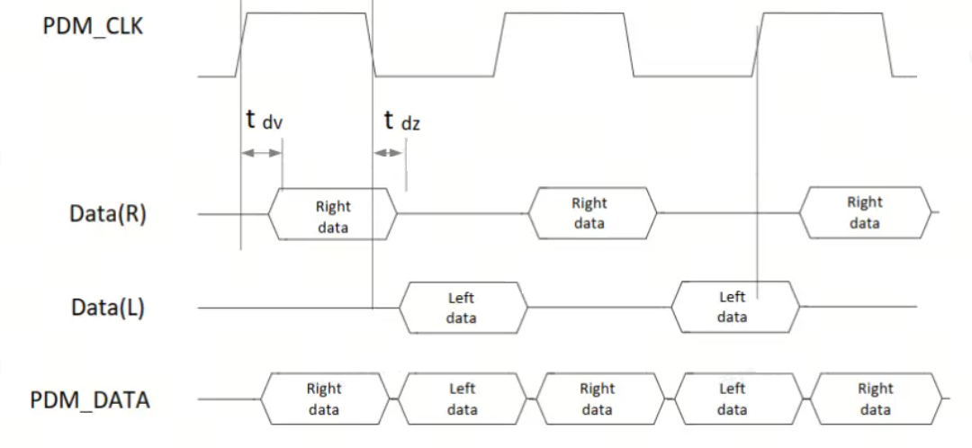
The PDM pin is multiplexed in AVDD18_PERI1 power domains, and operates at 1.8V level. It is necessary to verify the IO voltage levels of the PDM peripheral to match the corresponding IO power domain.
Recommendations
The recommended PDM0 design are shown in the table below.
| Signal | Power Domain | Connection Method | Description |
|---|---|---|---|
| PDM_CLK | AVDD18_PERI1 | Serial connection with 22ohm resistor | PDM clock |
| PDM_SDIN0 | Direct connection | PDM data input 0 | |
| PDM_SDIN1 | Direct connection | PDM data input 1 | |
| PDM_SDIN2 | Direct connection | PDM data input 2。 | |
| PDM_SDIN3 | Direct connection | PDM data input 3 |
When implementing board-to-board connections through connectors, it is recommended to use series resistors (between 22 ohms and 100 ohms, depending on SI testing requirements) and to reserve TVS components for both clock and control signals.
Audio Peripheral Design Reference
In most cases, the digital audio interfaces mentioned above cannot be used directly and must be paired with relevant peripherals to implement specific audio functionalities. In this section, design suggestions are provided for common audio scenarios that users can refer to.
Playback Devices, Headphones, Speakers
For speaker playback requirements, the following implementation options are available. A210 can be connected to audio DAC via I2S to achieve analog output, and then drive the speakers through an audio amplifier for power amplification.
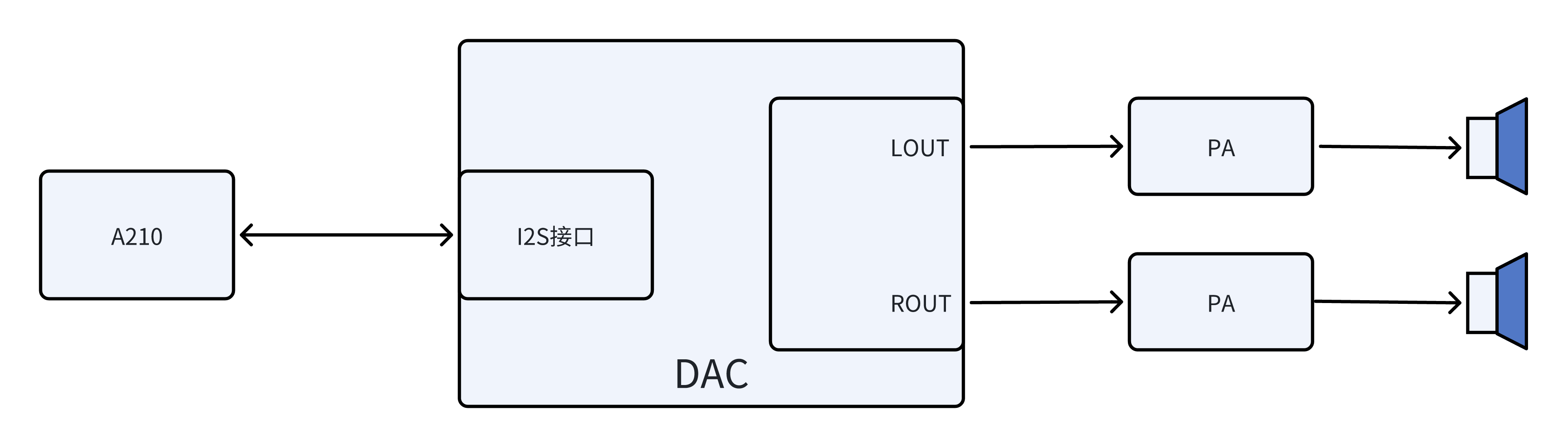
Recording Devices, Microphones
In applications such as tablets and laptops, there is a need for both playback and recording. In such cases, an integrated codec with ADC and DAC is typically used to achieve the required functionality, as shown in the diagram below.
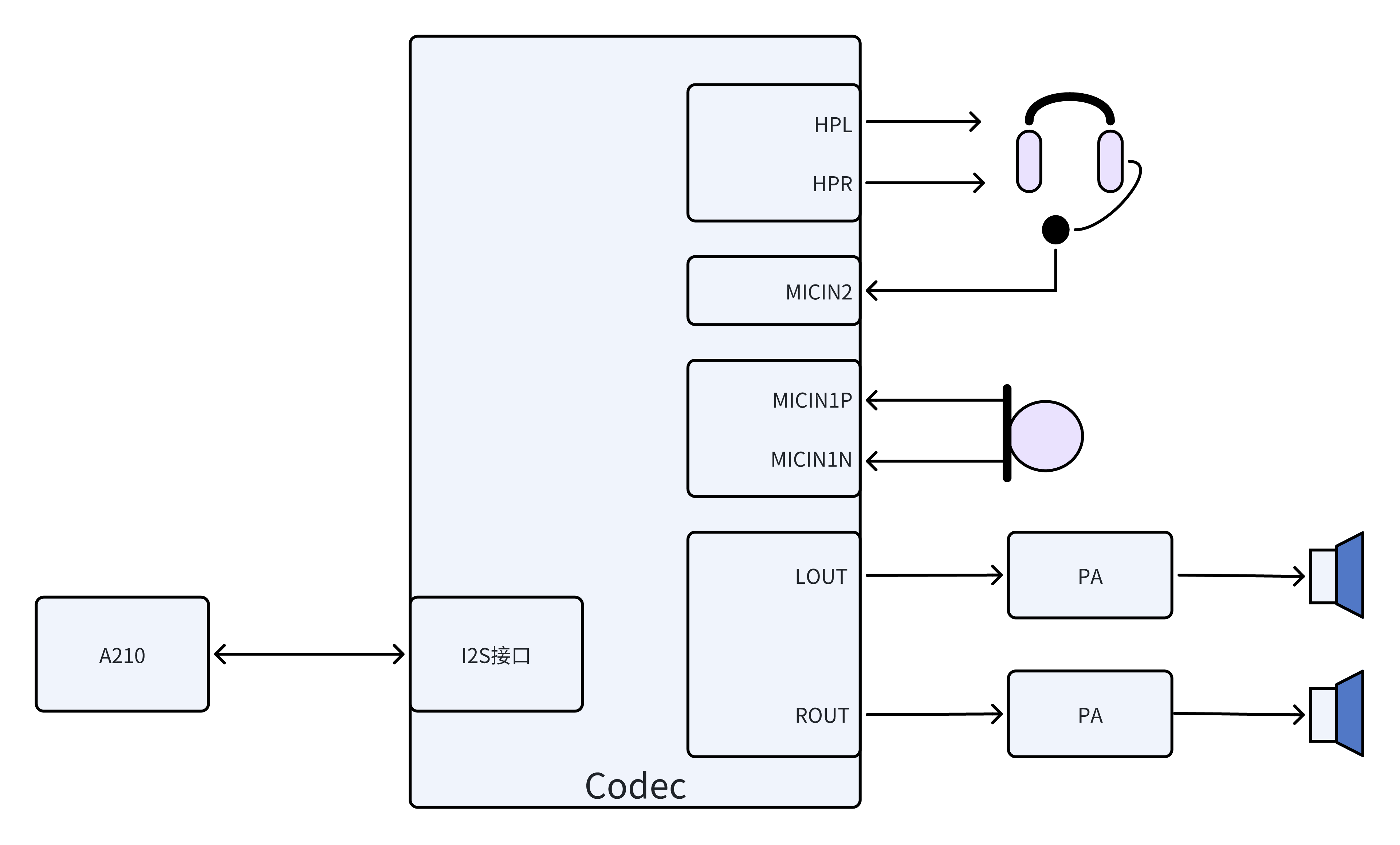
Introduction to Multi-Microphone Solutions
For scenarios that require multiple microphone inputs (microphone arrays, far-field reC0Gnition), there are three common expansion methods. If none of three options meet your specific requirements, please contact technical support to discuss feasibility.
- Multiple microphones and speaker capture can be achieved through a codec with a I2S interface.
- Multiple microphones and speaker capture can be achieved through a codec with a PDM interface.
- Recording can be done using microphones with a PDM interface, while speaker capture can be achieved through a codec with a PDM interface.
If there is a lack of available channels, multiple SDI data lines can be used to achieve multi-channel input, or cascaded input can be achieved through the TDM mode of the I2S interface. Simply stack identical circuits in hardware.
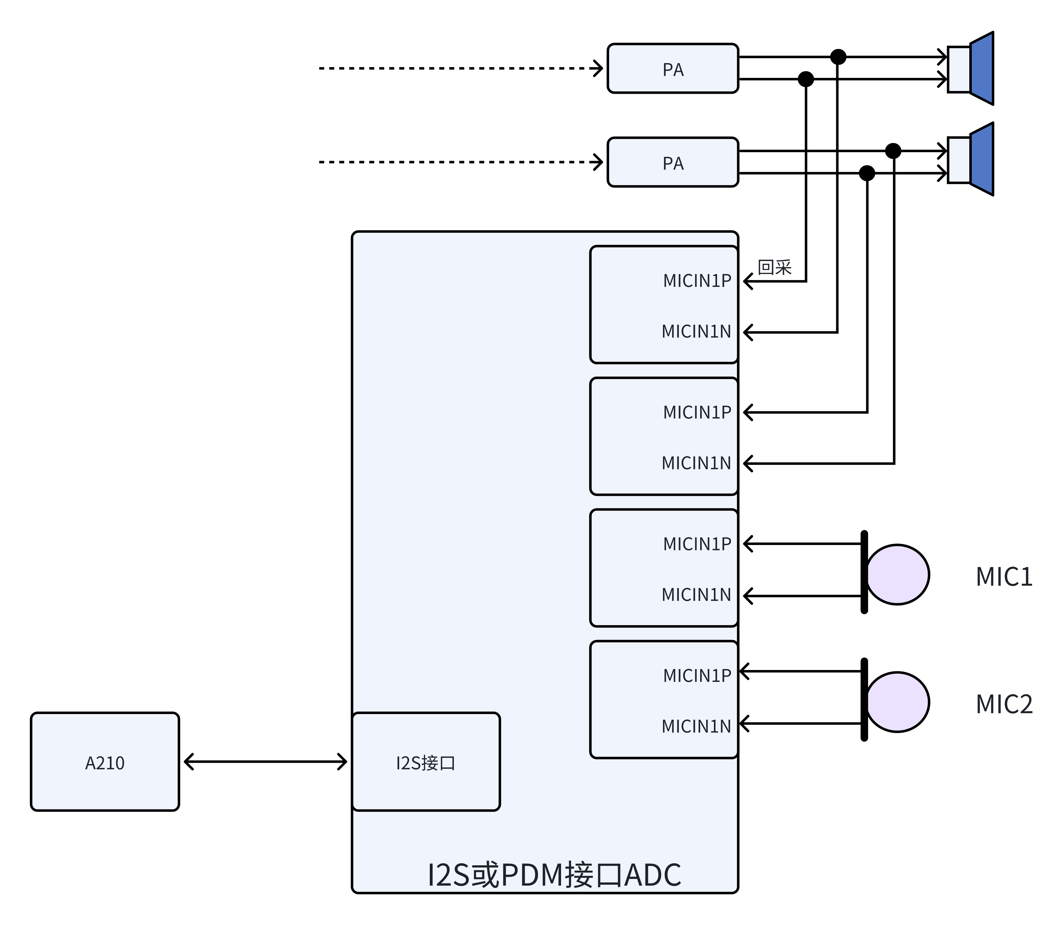
GMAC Interface Circuit
Overview
The A210 chip has two GMAC controllers that provide RMII or RGMII interfaces to connect to external Ethernet PHYs. The GMAC controllers support the following functionalities.
- RGMII interface with data transfer rates of 10/100/1000 Mbps.
- Supports TSN.
- Supports TSO.
- Supports GMAC Virtualization (Multiple Channels and Queues).
- Supports UFO.
- Supports hardware flow control.
- Supports remote wake-up
GMAC0 and GMAC1 are multiplexed in AVDD18_PERI1 power domains.
Recommendations
Considerations for RGMII interface design.
-
GMAC0 and GMAC1 only supports 1.8V voltage levels.
-
The decoupling capacitors for the VCCIOx_VCC power supplies of the RGMII/RMII interfaces should not be removed. Place them close to the pins during layout.
-
TXD0-TXD3, TXCLK and TXEN should have a 0-ohm resistor reserved on the A210 side to improve signal quality if necessary.
-
RXD0-RXD3, RXCLK and RXDV should have 22-ohm resistors connected on the PHY side to improve signal quality.
-
The recommended pull-up/pull-down and matching design for RGMII interfaces as follow table.
Signal IO Type (Chip side) Connection Method RGMII Interface Description GMACx_TX_CLK O Serial connection with 27ohm resistor, close to A210 RGMIIx_TX_CLK Data transmit reference clock GMACx_RX_CLK I Serial connection with 22ohm resistor, close to PHY RGMIIx_RX_CLK Data receive reference clock GMACx_TXEN O Serial connection with 27ohm resistor, close to A210 RGMIIx_TXEN Data transmit enable (rising edge)
Data transmit error (falling edge)
GMACx_TXD[3:0] O Serial connection with 27ohm resistor, close to A210 RGMIIx_TXD[3:0] Data transmit GMACx_RXDV I Serial connection with 22ohm resistor, close to PHY RGMIIx_RXDV Data receive valid (rising edge)
Data receive Error (falling edge)
GMACx_RXD[3:0] I Serial connection with 22ohm resistor, close to PHY RGMIIx_RXD[3:0] Data receive GMACx_MDC O Serial connection with 27ohm resistor, close to A210 RGMIIx_MDC Management data clock GMACx_MDIO I/O External pull-up with 1.5Kohm resistor RGMIIx_MDIO Management data output/input GMACx_PHY_INT I RGMIIx_INTB Interrupt and wake-up signal input GMAC0_EPHY_CLK O Reserved with 0-ohm resistor, close to A210 RGMIIx_EXT_CLK A210 provides 25MHz clock instead of PHY crystal -
When board-to-board connection is realized through the connector, it is recommended to connect a resistor in series (between 22ohm-100ohm, subject to the ability to satisfy the SI test) and to reserve a TVS device.
-
RGMII connection diagram is shown in the figure below, please see the reference diagram for the specific circuit (GEPHY working clock uses an external 25MHz crystal):
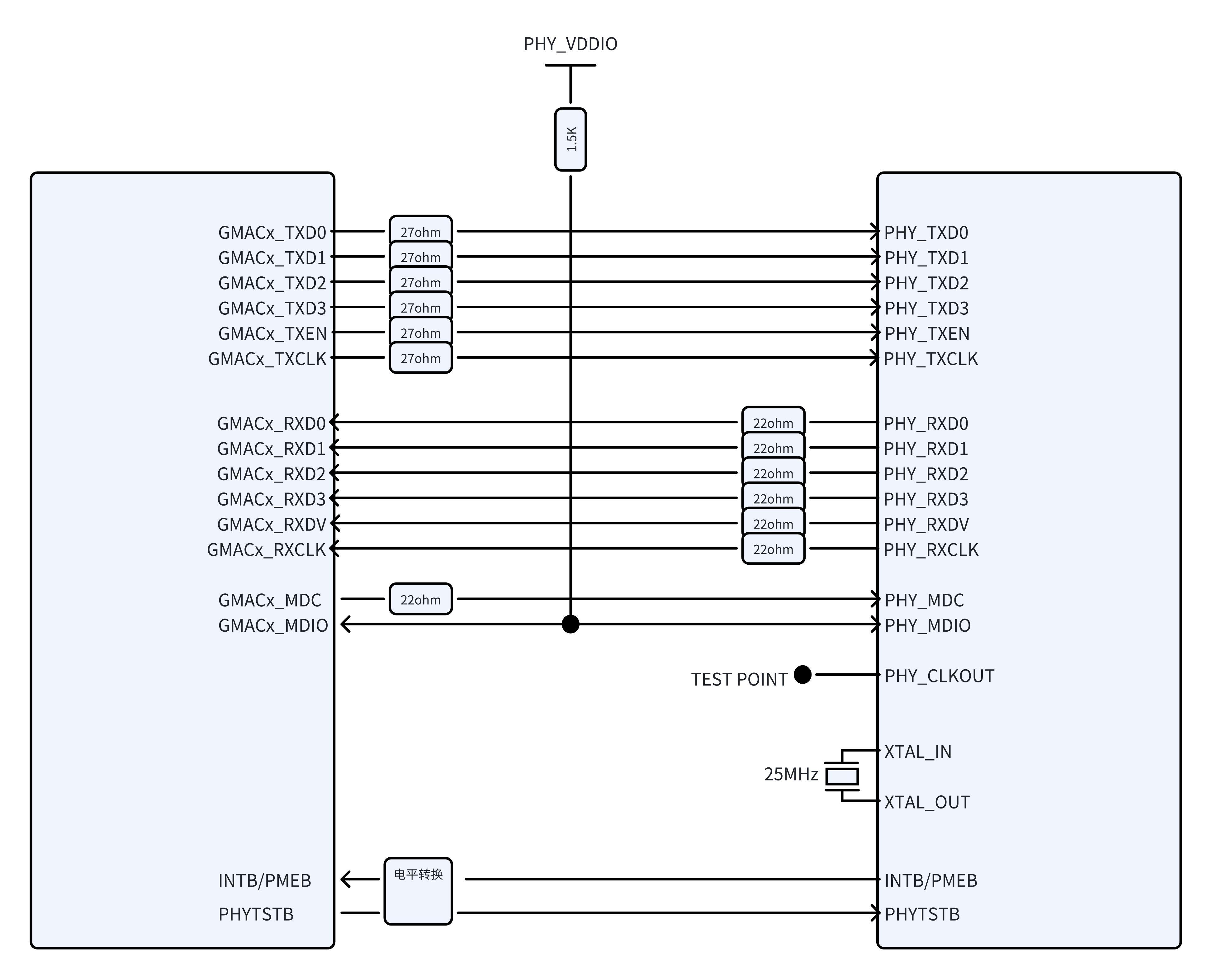
-
RGMII connection diagram is shown in the figure below, please see the reference diagram for specific circuitry (GEPHY working clock uses 25MHz provided by A210).
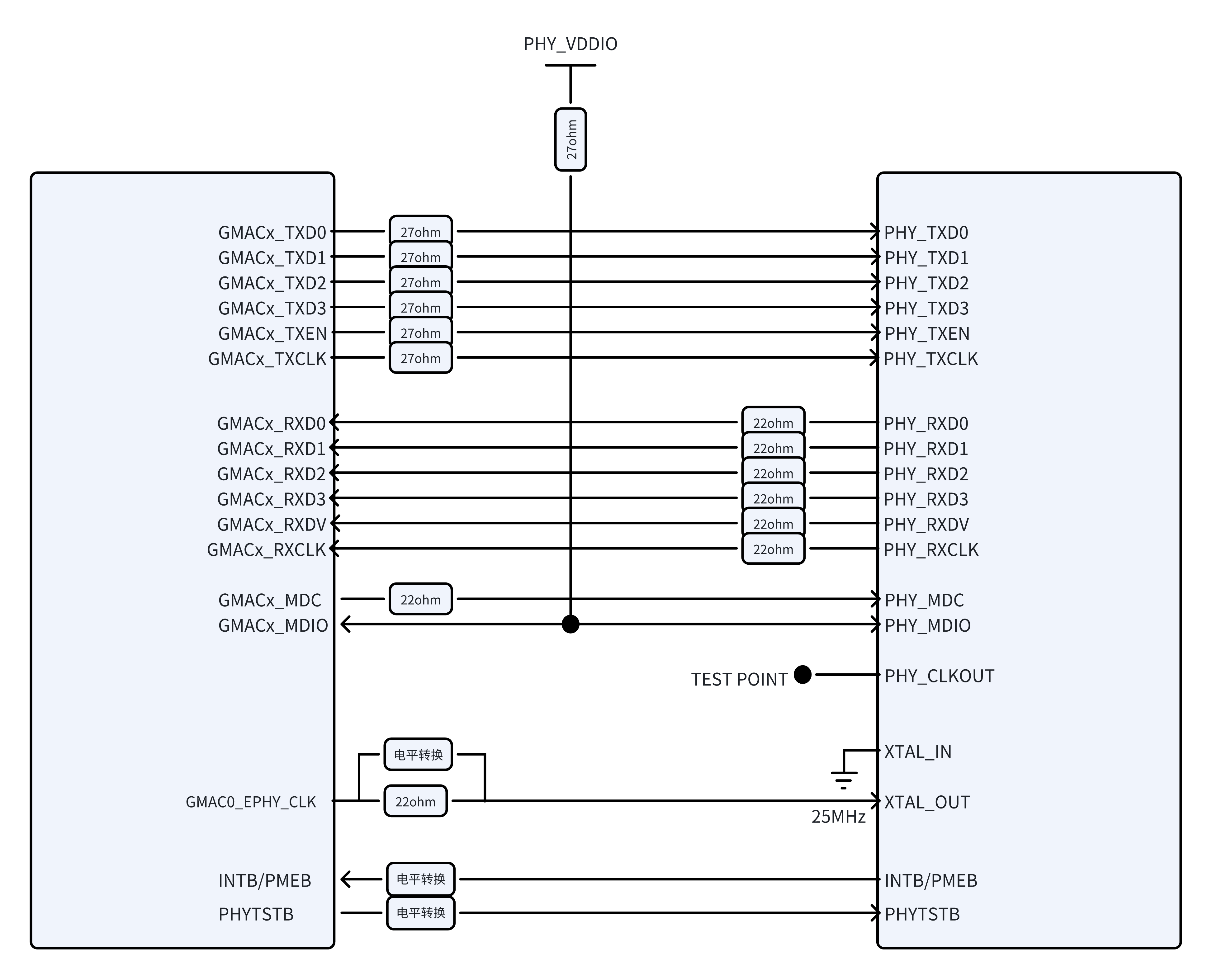
-
The Reset signal of the Ethernet PHY needs to be controlled by GPIO, and the GPIO level must match the PHY IO level. A 100nF capacitor should be added near the PHY pins to enhance electrostatic protection.
Caution:
The reset pin of RTL8211F/FI only supports a 3.3V level, therefore a level conversion circuit is required.
-
INTB/PMEB signal of Ethernet PHY is connected to the A210 GMACx_PHY_INT. If wake-up functionality is required, the signal can also be connected to an AON GPIO. The signal level voltage is 1.8V and please ensure the PHY IO level match.
Caution:
INTB/PMEB of RTL8211F/FI is an open-drain output and an external pull-up resistor must be added.
-
When using an external crystal for the PHY, select the capacitance value of the crystal according to the actual load capacitance, keeping the frequency offset within +/-20ppm.
-
MDIO requires an external pull-up resistor, recommended value is 1.5 to 1.8Kohm, and the pull-up voltage must match the IO voltage.
-
The connection of the center tap of the Ethernet PHY transformer is recommended to refer to the reference design provided by the respective PHY manufacturer, as different PHY manufacturers may have different connection methods.
-
For the 1000pF isolation capacitor, it is recommended to use a high-voltage safety capacitor with sufficient electrical clearance to ensure lightning protection.
-
The 75-ohm resistor on the high-voltage side of the network transformer should be in a package size of 0805 or above.
-
To achieve a lightning protection level of 4KV or above, additional surge protectors are required. Ordinary isolation transformers can only meet the 2KV level requirement.
-
If there are requirements for differential testing against lightning strikes, TVS diodes need to be added to the MDI differential pairs.
-
The hardware configuration for PHY initialization must match the actual requirements.
UART Interface Circuit
The A210 chip features 12 UART controllers, including one AO UART and 10 general UAARTs。
The specific distribution of UART interfaces on the A210 is as follows.
| UART NO. | UART Signal | Power Domain | Remarks |
|---|---|---|---|
| AOUART | AOUART_TXD | AVDD18_AON | E902 debug UART. Recommended to reserve. |
| AOUART_RXD | |||
| UART0 | UART0_TXD | AVDD18_PERI1 | |
| UART0_RXD | |||
| UART0_CTSN | |||
| UART0_RTSN | |||
| UART1 | UART1_TXD | ||
| UART1_RXD | |||
| UART2 | UART2_TXD | ||
| UART2_RXD | |||
| UART3 | UART3_TXD | ||
| UART3_RXD | |||
| UART4 | UART4_TXD | AVDD18_PERI2 | C908/C920 debug UART. Recommended to reserve. |
| UART4_RXD | |||
| UART5 | UART5_TXD | ||
| UART5_RXD | |||
| UART6 | UART6_TXD | ||
| UART6_RXD | |||
| UART6_CTSN | |||
| UART6_RTSN | |||
| UART7 | UART7_TXD | Can be used for IRDA | |
| UART7_RXD | |||
| UART8 | UART8_TXD | ||
| UART8_RXD | |||
| UART9 | UART9_TXD | ||
| UART9_RXD |
- UART signals all operate at 1.8V and should be pay attention to its level must be match the peripherals. A level conversion circuit is required when the level mismatch.
- AOUART and UART4 are the debug UARTs by default. Recommended to reserve.
- When implementing board-to-board connections through connectors, it is recommended to reserve TVS devices.
- The UART supports Infrared (IR) mode and can be connected to an IRDA Transceiver to enable infrared transmit and receive functionality. It is recommended to use UART7.
SPI Interface Circuit
In addition to the two FSPI controllers, the A210 chip has three general-purpose SPI controllers, including one AO SPI and two ordinary SPIs.
- Support for master modes.
- AO SPI supports low-power wake-up.
- Supports two chip selects for each port.
The distribution of SPI interfaces is as follows.
| SPI NO. | Signal | Power Domain |
|---|---|---|
| AOSPI | AOSPI_CSN0 | AVDD18_AON |
| AOSPI_CSN1 | ||
| AOSPI_D0_MOSI | ||
| AOSPI_D1_MISO | ||
| AOSPI_SCLK | ||
| SPI0 | SPI0_CSN0 | AVDD18_PERI1 |
| SPI0_CSN1 | ||
| SPI0_D0_MOSI | ||
| SPI0_D1_MISO | ||
| SPI0_SCLK | ||
| SPI1 | SPI1_CSN0 | AVDD18_PERI2 |
| SPI1_CSN1 | ||
| SPI1_D0_MOSI | ||
| SPI1_D1_MISO | ||
| SPI1_SCLK |
- The SPI signals all operate at 1.8V and should be pay attention to its level must be match the peripherals. A level conversion circuit is required when the level mismatch.
- When implementing board-to-board connections through connectors, it is recommended to reserve TVS devices.
CAN Interface Circuit
The A210 chip has 3 CAN controllers.
The distribution of CAN interfaces on the A210 chip is as follows.
| CAN NO. | Signal | Power Domain |
|---|---|---|
| CAN0 | CAN0_RX | AVDD18_PERI1 |
| CAN0_TX | ||
| CAN1 | CAN1_RX | |
| CAN1_TX | ||
| CAN2 | CAN2_RX | AVDD18_PERI2 |
| CAN2_TX |
- The CAN signals all operate at 1.8V and should be pay attention to its level must be match the peripherals. A level conversion circuit is required when the level mismatch.
- When implementing board-to-board connections through connectors, it is recommended to reserve TVS devices.
I2C Interface Circuit
The A210 chip features 10 I2C controllers that support the following features.
- Support for I2C bus master mode.
- Maximum data rate: 3.4Mbps.
- Support for 7-bit and 10-bit addressing modes.
10 IC controllers include 2 AO I2Cs (supporting wake-up functionality) and 8 general-purpose I2Cs.
The distribution of I2C interfaces on the A210 chip is provided in the following table.
| I2C NO. | Power Domain |
|---|---|
| AOI2C0 | AVDD18_AON |
| AOI2C1 | |
| I2C0 | AVDD18_PERI1 |
| I2C1 | |
| I2C2 | |
| I2C3 | AVDD18_PERI2 |
| I2C4 | |
| I2C5 | |
| I2C6 | |
| I2C7 |
- The I2C signals all operate at 1.8V and should be pay attention to its level must be match the peripherals. A level conversion circuit is required when the level mismatch.
- The I2C signals SCL and SDA require external pull-up resistors. Select the appropriate resistor value based on the bus load.
- Ensure that the addresses of different devices on the I2C bus do not conflict, and the pull-up power supply must be consistency.
- When implementing board-to-board connections through connectors, it is recommended to reserve TVS devices.
PWM Interface Circuit
The RK3576 chip integrates 3 independent PWM controllers, supporting a maximum of 16 PWM channels (8 channels per controller) with a maximum frequency of 12 MHz.
PWM 接口分布情况如下表所示。The distribution of PWM interfaces on the A210 chip is as follows:
| PWM NO. | Power Domain |
|---|---|
| PWM0_CH0 | AVDD18_PERI1 |
| PWM0_CH1 | |
| PWM0_CH2 | |
| PWM0_CH3 | |
| PWM0_CH4 | |
| PWM0_CH5 | |
| PWM1_CH0 | AVDD18_PERI2 |
| PWM1_CH1 | |
| PWM1_CH2 | |
| PWM1_CH3 | |
| PWM1_CH4 | |
| PWM1_CH5 | |
| PWM2_CH0 | AVDD18_PERI2 |
| PWM2_CH1 | |
| PWM2_CH2 | |
| PWM2_CH3 | |
| PWM2_CH4 | |
| PWM2_CH5 |
- The PWM signals all operate at 1.8V and should be pay attention to its level must be match the peripherals. A level conversion circuit is required when the level mismatch.
- When implementing board-to-board connections through connectors, it is recommended to serially connect resistors with a specific resistance value (between 22 ohms and 100 ohms, depending on meeting SI testing requirements) and reserve TVS (Transient Voltage Suppression) devices.
C2C
The C2C (Chip-to-Chip) interface is designed to achieve tight coupling by multiple chip interconnection, thereby enhancing overall computational capabilities.
The A210 supports 2 C2C ports, one of which supports cache coherent interconnect.
- Each C2C port provides a bandwidth of ≥20 GB/s. Under a 128B@BL payload, the read/write bandwidth utilization is ≥71%.
- Supports lane swapping between the two C2C ports.
The C2C topology varies depending on the number of chips integrated into the system.
-
1-Chip
In a single-chip scenario, the C2C module is not required. The external C2C pins should be pulled down to Ground (GND) as shown below.
-
2-Chip
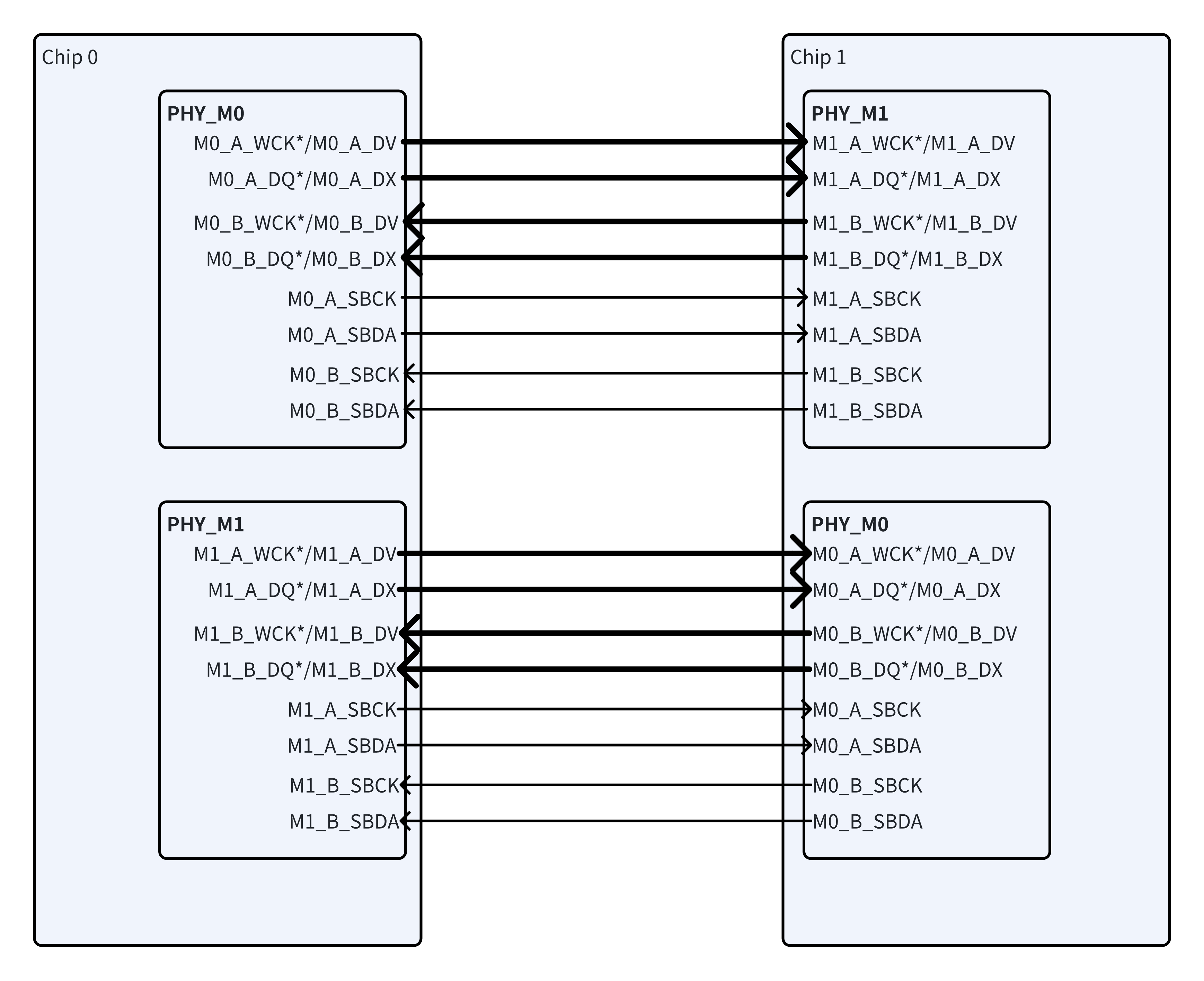
-
4-Chip